

| Distributor | Stock | Pricing | MOQ | PKG | Lead Time | Date Code | On Order Quantity | On Order Delivery | |
|---|---|---|---|---|---|---|---|---|---|
|
7,431 pcs
|
7431 pcs | On Request | 1 | On Request | On Request | 12+ | On Request | On Request | |
|
673 pcs
|
673 pcs | On Request | 1 | On Request | On Request | On Request | On Request | On Request | |
|
22 pcs
|
22 pcs | On Request | 1 | On Request | On Request | 1116 | On Request | On Request |
| Category | |
| Manufacturer Name | |
| Lead Spacing | |
| Mounting Type | |
| Number of I | |
| Number of LABs | |
| Number of Logic Elements | |
| Operating Temperature | |
| Supplier Device Package | |
| Tape & Reel | |
| Total RAM Bits | |
| Voltage |
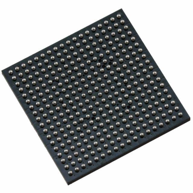
The Lattice Semiconductor LCMXO2280C-3FTN324I is a field programmable gate array (FPGA) designed for embedded systems. It features 2280 logic elements, 285 logic array blocks, and a total of 28.262 Kbits of RAM. The device supports 271 I/O pins and operates within a voltage range of 1.71V to 3.465V, with an operating temperature range from -40°C to 100°C. It is packaged in a 324-FTBGA (19x19) surface-mount package, making it suitable for compact and high-density applications. The FPGA includes two PLLs, embedded block RAM, distributed RAM, and supports various I/O buffer interfaces such as LVCMOS, LVTTL, PCI, LVDS, and LVPECL. It also supports IEEE Standard 1149.1 boundary scan and IEEE 1532 in-system programming, ensuring ease of integration and programming in embedded designs.
The FPGA has 2280 logic elements.
The FPGA supports 271 I/O pins.
The operating voltage range is 1.71V to 3.465V.
The FPGA is packaged in a 324-FTBGA (19x19).