

| Distributor | Stock | Pricing | MOQ | PKG | Lead Time | Date Code | On Order Quantity | On Order Delivery | |
|---|---|---|---|---|---|---|---|---|---|
|
10 pcs
|
10 pcs | On Request | 1 | On Request | On Request | On Request | On Request | On Request |
| Category | |
| Manufacturer Name | |
| Halogen Free | |
| Lead Spacing | |
| Mounting Type | |
| Number of I | |
| Number of LABs | |
| Number of Logic Elements | |
| Operating Temperature | |
| Supplier Device Package | |
| Total RAM Bits | |
| Voltage |
The Lattice Semiconductor LCMXO2-7000ZE-3TG144C is a member of the MachXO2 family of ultra-low power, instant-on, non-volatile Programmable Logic Devices (PLDs). This FPGA features a flexible logic architecture with 6864 LUTs and 114 I/O pins, making it suitable for a wide range of applications.
Key features include embedded block RAM (EBR) with up to 240 Kbits and distributed RAM up to 54 Kbits, along with 256 Kbits of on-chip user flash memory. The device operates at a voltage range of 1.14V to 1.26V and supports various I/O interfaces such as LVCMOS, LVTTL, LVDS, and HSTL.
Designed for low power consumption, the MachXO2 family utilizes an advanced 65 nm process, with standby power as low as 19 µW. The device is non-volatile and infinitely reconfigurable, offering instant-on capability and secure solutions. It supports multiple programming interfaces including JTAG, SPI, and I2C.
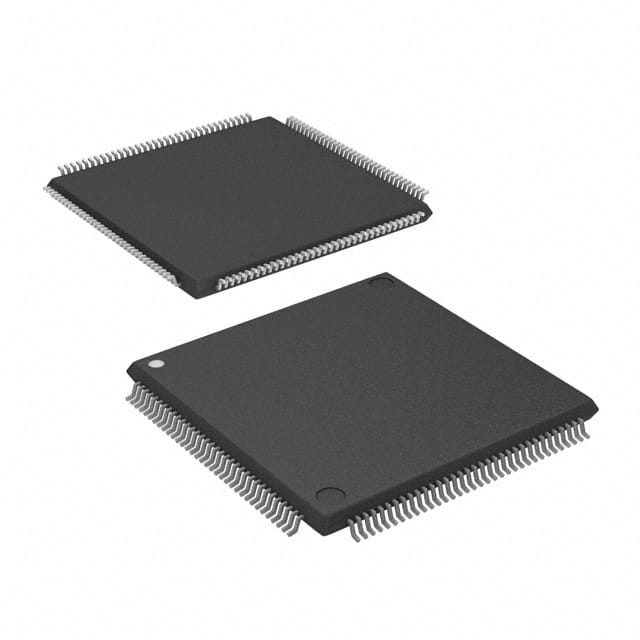
The LCMXO2-7000ZE-3TG144C comes in a 144-TQFP package and is surface mountable. It operates within a temperature range of 0°C to 85°C (TJ). The advanced halogen-free packaging ensures environmental compliance.
The LCMXO2-7000ZE-3TG144C features 6864 LUTs and 858 LABs.
This FPGA has 114 I/O pins.
The operating voltage is between 1.14V and 1.26V.
It is supplied in a 144-TQFP (20x20) package and also listed as 144-LQFP.
The standby power consumption is as low as 19 µW.
It offers up to 240 Kbits of sysMEM Embedded Block RAM and up to 54 Kbits of Distributed RAM.
Yes, it has up to 256 Kbits of User Flash Memory with 100,000 write cycles.