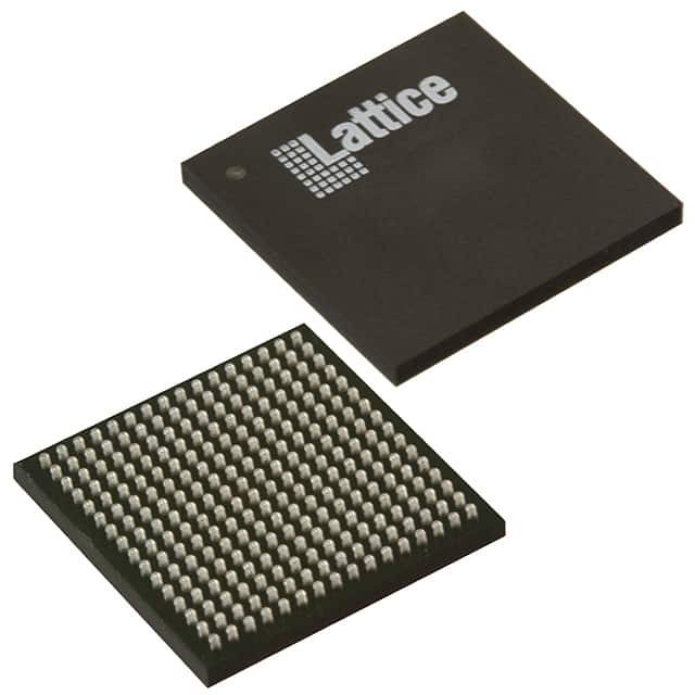
The Lattice Semiconductor LCMXO2-7000HE-5BG256C is a Field Programmable Gate Array (FPGA) from the MachXO2 family. This device features 6864 logic elements and 858 logic block arrays, providing a flexible architecture for various digital applications.
It offers 206 programmable input/output pins and includes 245760 bits of total RAM. The operating supply voltage ranges from 1.14V to 1.26V, with an operating temperature range of 0°C to 85°C (TJ). The FPGA is housed in a 256-CABGA (14x14) package, suitable for surface mount applications.
Key features include its non-volatile, infinitely reconfigurable nature, with instant-on capability. The MachXO2 family utilizes an advanced 65 nm low power process. This specific device is designed for general-purpose logic control in embedded systems, consumer electronics, industrial control, data processing, and communications equipment.