

| Distributor | Stock | Pricing | MOQ | PKG | Lead Time | Date Code | On Order Quantity | On Order Delivery | |
|---|---|---|---|---|---|---|---|---|---|
|
579 pcs
|
579 pcs | On Request | 1 | On Request | On Request | On Request | On Request | On Request |
| Category | |
| Manufacturer Name | |
| Lead Spacing | |
| Mounting Type | |
| Number of I | |
| Number of LABs | |
| Number of Logic Elements | |
| Operating Temperature | |
| Supplier Device Package | |
| Supplier Package | |
| Total RAM Bits | |
| Voltage |
The Lattice Semiconductor LCMXO2-640UHC-6TG144I is a member of the MachXO2 family of Field Programmable Gate Arrays (FPGAs). This device offers 640 logic elements and 107 I/O pins, making it suitable for a variety of embedded applications.
Key electrical specifications include 65536 total RAM bits and an operating voltage range of 2.375V to 3.465V. The device operates within a temperature range of -40°C to 100°C (TJ).
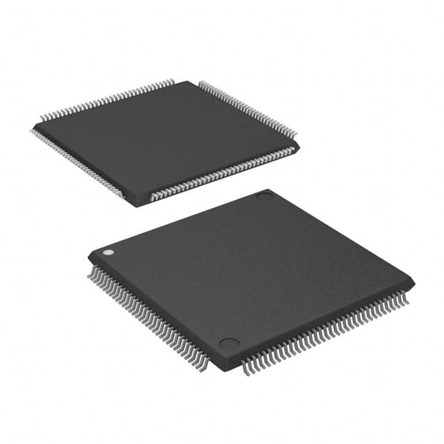
This FPGA is designed for surface mounting and comes in a 144-LQFP package. The MachXO2 family utilizes a 65 nm low power process and offers features such as on-chip user flash memory and embedded memory blocks.
Additional features from the datasheet include up to 256 kbits of user flash memory with 100,000 write cycles, and up to 240 kbits of embedded block RAM. The device also supports low standby power consumption, as low as 22 µW.
The LCMXO2-640UHC-6TG144I FPGA features 640 logic elements, 107 I/O pins, and 65536 total RAM bits. It operates within a voltage range of 2.375V to 3.465V.
The operating temperature range for the LCMXO2-640UHC-6TG144I FPGA is -40°C to 100°C (TJ).
This FPGA is supplied in a 144-LQFP package and is designed for surface mounting.
Yes, the LCMXO2-640UHC-6TG144I FPGA has up to 256 kbits of on-chip user flash memory.
The device offers up to 240 kbits of sysMEM™ Embedded Block RAM.