

| Distributor | Stock | Pricing | MOQ | PKG | Lead Time | Date Code | On Order Quantity | On Order Delivery | |
|---|---|---|---|---|---|---|---|---|---|
|
684 pcs
|
684 pcs | On Request | 1 | On Request | On Request | On Request | On Request | On Request |
| Category | |
| Manufacturer Name | |
| Lead Spacing | |
| Mounting Type | |
| Number of I | |
| Number of LABs | |
| Number of Logic Elements | |
| Operating Temperature | |
| Supplier Device Package | |
| Supplier Package | |
| Total RAM Bits | |
| Voltage |
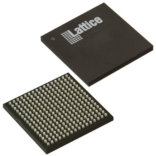
The Lattice Semiconductor LCMXO2-4000HC-5BG256C is an FPGA from the MachXO2 family, designed for flexible logic implementation. It offers 4320 logic elements and 540 LABs, supported by 94208 total RAM bits. The device provides 206 I/O pins and operates on a supply voltage ranging from 2.375V to 3.465V.
This FPGA is suitable for applications requiring embedded memory, with up to 240 kbits of sysMEM™ Embedded Block RAM and 54 kbits of Distributed RAM. It also includes up to 256 kbits of on-chip user flash memory with 100,000 write cycles, accessible via WISHBONE, SPI, I2C, and JTAG interfaces.
The device operates within a temperature range of 0°C to 85°C (TJ) and is available in a 256-LFBGA or 256-CABGA package. It is designed for surface mounting, making it adaptable for various PCB designs. The MachXO2 family is known for its ultra-low power consumption, with standby power as low as 22 µW.
Key features include flexible I/O buffers supporting a wide range of interfaces, on-chip clocking capabilities with up to two analog PLLs, and non-volatile, infinitely reconfigurable architecture with instant-on functionality. These characteristics make it a versatile component for embedded systems.
The LCMXO2-4000HC-5BG256C FPGA has 4320 logic elements.
The LCMXO2-4000HC-5BG256C FPGA has 206 I/O pins.
The operating voltage range for the LCMXO2-4000HC-5BG256C FPGA is 2.375V to 3.465V.
The LCMXO2-4000HC-5BG256C FPGA is available in a 256-LFBGA and 256-CABGA package.
The operating temperature range for the LCMXO2-4000HC-5BG256C FPGA is 0°C to 85°C (TJ).
The LCMXO2-4000HC-5BG256C FPGA has 94208 total RAM bits.
Yes, the LCMXO2-4000HC-5BG256C FPGA has up to 256 kbits of on-chip user flash memory.