

| Distributor | Stock | Pricing | MOQ | PKG | Lead Time | Date Code | On Order Quantity | On Order Delivery | |
|---|---|---|---|---|---|---|---|---|---|
|
40 pcs
|
40 pcs | On Request | 1 | On Request | On Request | On Request | On Request | On Request |
| Category | |
| Manufacturer Name | |
| Mounting Type | |
| Number of I | |
| Number of LABs | |
| Number of Logic Elements | |
| Operating Temperature | |
| Supplier Device Package | |
| Supplier Package | |
| Tape & Reel | |
| Voltage |
The Lattice Semiconductor Corporation LCMXO2-256HC-5SG48C is an FPGA from the MachXO2 family. It offers a flexible logic architecture with 256 LUTs and 32 LABs, supporting 40 I/O pins. This device operates within a voltage range of 2.375V to 3.465V and has an operating temperature range of 0°C to 85°C (TJ).
Key features include embedded memory with up to 256 kbits of User Flash Memory, 240 kbits of sysMEM™ Embedded Block RAM, and 54 kbits of Distributed RAM. The I/O buffer supports a wide range of interfaces, including LVCMOS, LVTTL, LVDS, and others. It also includes up to two analog PLLs with a wide input frequency range from 7 MHz to 400 MHz.
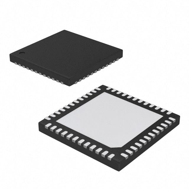
This FPGA is designed for surface mounting and comes in a 48-VFQFN exposed pad package (Supplier Package: 48-QFNS (7x7)). Its non-volatile, infinitely reconfigurable nature allows for instant-on functionality, powering up in microseconds. The device is programmable through JTAG, SPI, or I2C interfaces.
The LCMXO2-256HC-5SG48C FPGA has 256 logic elements.
The LCMXO2-256HC-5SG48C has 40 I/O pins.
The operating voltage range for the LCMXO2-256HC-5SG48C is 2.375V to 3.465V.
The LCMXO2-256HC-5SG48C is supplied in a 48-VFQFN Exposed Pad package.
The operating temperature for the LCMXO2-256HC-5SG48C is 0°C to 85°C (TJ).
Yes, the LCMXO2-256HC-5SG48C features up to 256 kbits of User Flash Memory.