

| Distributor | Stock | Pricing | MOQ | PKG | Lead Time | Date Code | On Order Quantity | On Order Delivery | |
|---|---|---|---|---|---|---|---|---|---|
|
168 pcs
|
168 pcs | On Request | 1 | On Request | On Request | 1970-01-03 07:57:06 | On Request | On Request |
| Category | |
| Manufacturer Name | |
| Lead Spacing | |
| Mounting Type | |
| Number of I | |
| Number of LABs | |
| Number of Logic Elements | |
| Operating Temperature | |
| Supplier Device Package | |
| Voltage |
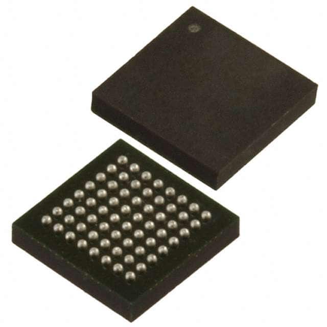
The Lattice Semiconductor LCMXO2-256HC-4UMG64I is a Field Programmable Gate Array (FPGA) designed for flexible logic implementation. It offers 256 logic elements and 32 logic array blocks, providing a capacity for complex digital designs.
This FPGA supports 44 I/O pins, allowing for extensive interfacing with other components. It operates within a voltage range of 2.375V to 3.465V and has an operating temperature range of -40°C to 100°C (TJ), making it suitable for various environmental conditions.
The device is designed for surface mounting, utilizing a 64-UCBGA (4x4) package. Its features include ultra-low power consumption and non-volatile configuration, enabling instant-on functionality.
Key specifications include 256 LUTs (LUT4s), up to 240 kbits of embedded block RAM, and up to 54 kbits of distributed RAM. It also includes up to 256 kbits of on-chip user flash memory with 100,000 write cycles, accessible via WISHBONE, SPI, I2C, and JTAG interfaces.
The LCMXO2-256HC-4UMG64I has 256 logic elements.
The LCMXO2-256HC-4UMG64I has 44 I/O pins.
The operating voltage range for the LCMXO2-256HC-4UMG64I is 2.375V to 3.465V.
The operating temperature range for the LCMXO2-256HC-4UMG64I is -40°C to 100°C (TJ).
The LCMXO2-256HC-4UMG64I is supplied in a 64-UCBGA (4x4) package.