

| Distributor | Stock | Pricing | MOQ | PKG | Lead Time | Date Code | On Order Quantity | On Order Delivery | |
|---|---|---|---|---|---|---|---|---|---|
|
250 pcs
|
250 pcs | On Request | 1 | On Request | On Request | On Request | On Request | On Request |
| Category | |
| Manufacturer Name | |
| Mounting Type | |
| Number of I | |
| Number of LABs | |
| Number of Logic Elements | |
| Operating Temperature | |
| Supplier Device Package | |
| Supplier Package | |
| Tape & Reel | |
| Total RAM Bits | |
| Voltage |
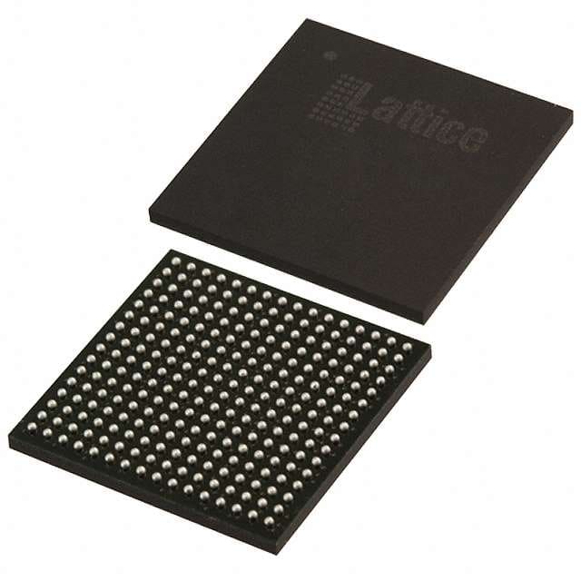
The Lattice Semiconductor LCMXO2-2000ZE-3FTG256I is a Field Programmable Gate Array (FPGA) integrated circuit from the MachXO2 family. It offers 2112 logic elements and 264 logic array blocks, providing flexible logic architecture.
This FPGA IC features 75776 total RAM bits and supports 206 I/O pins. It operates within a voltage range of 1.14V to 1.26V and has an operating temperature range of -40°C to 100°C (TJ). The device is suitable for various interfaces, including LVCMOS, LVDS, and HSTL.
Designed for surface mount applications, the LCMXO2-2000ZE-3FTG256I comes in a 256-LBGA package. It also includes features like up to 256 kbits of user flash memory and up to 240 kbits of embedded block RAM, making it a versatile solution for embedded systems.
The LCMXO2-2000ZE-3FTG256I features 2112 logic elements, 264 LABs, 75776 total RAM bits, and 206 I/O pins. It operates at a voltage range of 1.14V to 1.26V.
The operating temperature range for the LCMXO2-2000ZE-3FTG256I is -40°C to 100°C (TJ).
This FPGA is available in a 256-LBGA package and is designed for surface mount.
The MachXO2 family offers up to 256 kbits of user flash memory and up to 240 kbits of sysMEM™ embedded block RAM, along with up to 54 kbits of distributed RAM.
The programmable sysIO™ buffer supports a wide range of interfaces including LVCMOS 3.3/2.5/1.8/1.5/1.2, LVTTL, PCI, LVDS, Bus-LVDS, MLVDS, RSDS, LVPECL, SSTL 25/18, and HSTL 18.