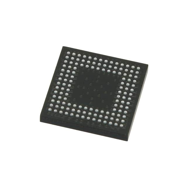
The Lattice Semiconductor LCMXO2-2000HE-6MG132I is a Field Programmable Gate Array (FPGA) from the MachXO2 family. It features a flexible logic architecture with 2112 logic elements and 264 LABs, supporting up to 104 I/O pins. This device offers 75776 total RAM bits and includes embedded and distributed memory options, with up to 240 kbits of sysMEM™ Embedded Block RAM and up to 54 kbits of Distributed RAM.
Designed for ultra-low power consumption, it utilizes an advanced 65 nm process and offers as low as 22 µW standby power. The FPGA includes on-chip user flash memory up to 256 kbits with 100,000 write cycles, accessible through WISHBONE, SPI, I2C, and JTAG interfaces. It supports a wide range of I/O interfaces, including LVCMOS, LVDS, and HSTL, with programmable sysIO™ buffers.
The device operates within a temperature range of -40°C to 100°C (TJ) and requires a voltage supply between 1.14V and 1.26V. It is packaged in a 132-LFBGA, CSPBGA format, specifically a 132-CSPBGA (8x8) with surface mount type. The FPGA is non-volatile and infinitely reconfigurable, offering instant-on capability in microseconds.