

| Distributor | Stock | Pricing | MOQ | PKG | Lead Time | Date Code | On Order Quantity | On Order Delivery | |
|---|---|---|---|---|---|---|---|---|---|
|
2,505 pcs
|
2505 pcs | On Request | 1 | On Request | On Request | On Request | On Request | On Request |
| Category | |
| Manufacturer Name | |
| Lead Spacing | |
| Mounting Style | |
| Mounting Type | |
| Number of I | |
| Number of LABs | |
| Number of Logic Elements | |
| Operating Temperature | |
| Supplier Device Package | |
| Tape & Reel | |
| Total RAM Bits | |
| Voltage |
The Lattice Semiconductor LCMXO2-2000HC-4TG144I is a Field Programmable Gate Array (FPGA) designed for flexible logic implementation. It features 2112 LUTs (Look-Up Tables) and provides 111 I/O pins, supporting a wide range of interfaces.
This device operates within a supply voltage range of 2.375V to 3.465V and has a maximum operating frequency of 133 MHz. It includes embedded memory options with 16 Kbit Distributed RAM, 74 Kbit Embedded Block RAM, and 80 Kbit User Flash Memory, totaling 170 Kbit of memory.
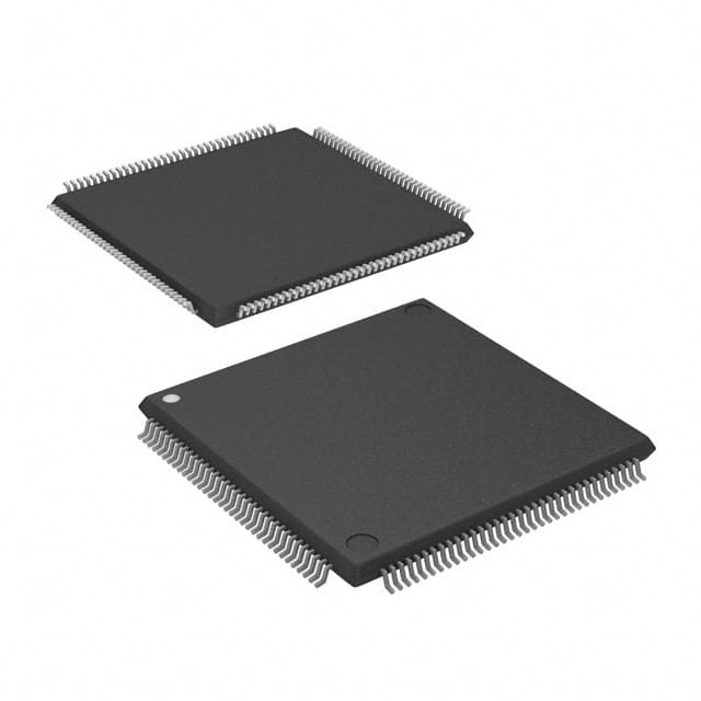
The LCMXO2-2000HC-4TG144I is supplied in a 144-TQFP package, suitable for surface mounting. It operates across a temperature range of -40°C to 100°C (TJ).
Key specifications include 264 LABs, a low operating supply current of 82 uA, and a total RAM bit count of 75776.
The LCMXO2-2000HC-4TG144I has 2112 logic elements.
The LCMXO2-2000HC-4TG144I features 111 I/O pins.
The operating supply voltage for the LCMXO2-2000HC-4TG144I is between 2.375V and 3.465V.
The LCMXO2-2000HC-4TG144I is supplied in a 144-TQFP (20x20) package.
The maximum operating frequency for the LCMXO2-2000HC-4TG144I is 133 MHz.
The LCMXO2-2000HC-4TG144I has 16 Kbit Distributed RAM, 74 Kbit Embedded Block RAM, and 80 Kbit User Flash Memory, for a total of 170 Kbit.