

| Distributor | Stock | Pricing | MOQ | PKG | Lead Time | Date Code | On Order Quantity | On Order Delivery | |
|---|---|---|---|---|---|---|---|---|---|
|
258 pcs
|
258 pcs | On Request | 1 | On Request | On Request | On Request | On Request | On Request |
| Category | |
| Manufacturer Name | |
| Mounting Type | |
| Number of I | |
| Number of LABs | |
| Number of Logic Elements | |
| Operating Temperature | |
| Supplier Device Package | |
| Supplier Package | |
| Tape & Reel | |
| Total RAM Bits | |
| Voltage |
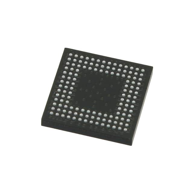
The Lattice Semiconductor LCMXO2-1200ZE-3MG132C is an FPGA from the MachXO2 family, designed for flexible logic implementation. It features 1280 logic elements and 160 Look-Up Tables (LUTs), providing significant processing capability.
This device offers 104 I/O pins and supports a wide range of interfaces. It includes 65536 bits of total RAM, with up to 240 kbits of embedded block RAM and up to 54 kbits of distributed RAM. The FPGA operates at a voltage range of 1.14V to 1.26V and has an operating temperature range of 0°C to 85°C.
With on-chip user flash memory of up to 256 kbits and 100,000 write cycles, this FPGA is non-volatile and infinitely reconfigurable. It supports instant-on functionality, powering up in microseconds. The device is housed in a 132-LFBGA, CSPBGA package and is designed for surface mounting.
Key features include ultra-low power consumption with as low as 22 µW standby power, flexible on-chip clocking, and pre-engineered source synchronous I/O. The MachXO2 family utilizes an advanced 65 nm low-power process.
The LCMXO2-1200ZE-3MG132C FPGA has 1280 logic elements.
The LCMXO2-1200ZE-3MG132C FPGA has 104 I/O pins.
The operating voltage range for the LCMXO2-1200ZE-3MG132C FPGA is 1.14V to 1.26V.
The LCMXO2-1200ZE-3MG132C FPGA is supplied in a 132-LFBGA, CSPBGA package.
The LCMXO2-1200ZE-3MG132C FPGA has 65536 total RAM bits.
The MachXO2 FPGA family has a standby power consumption as low as 22 µW.
The operating temperature range for the LCMXO2-1200ZE-3MG132C is 0°C to 85°C (TJ).