

| Distributor | Stock | Pricing | MOQ | PKG | Lead Time | Date Code | On Order Quantity | On Order Delivery | |
|---|---|---|---|---|---|---|---|---|---|
|
1,500 pcs
|
1500 pcs | On Request | 1 | On Request | On Request | On Request | On Request | On Request |
| Category | |
| Manufacturer Name | |
| Failure Rate | |
| Lead Spacing | |
| Mounting Type | |
| Number of I | |
| Number of LABs | |
| Number of Logic Elements | |
| Operating Temperature | |
| Operating Voltage | |
| Supplier Device Package | |
| Total RAM Bits | |
| Voltage |
The Lattice Semiconductor LCMXO1200E-5TN144C is a member of the MachXO family of FPGAs. This device offers 1200 logic elements and 150 LABs, supported by 9421 bits of RAM. It features 113 I/O pins and operates within a voltage range of 1.14V to 1.26V.
Designed for applications traditionally addressed by CPLDs and low-capacity FPGAs, such as glue logic, bus bridging, and control logic, this FPGA provides non-volatile, infinitely reconfigurable capabilities with instant-on performance. It supports a wide range of interfaces through its programmable sysIO buffer.
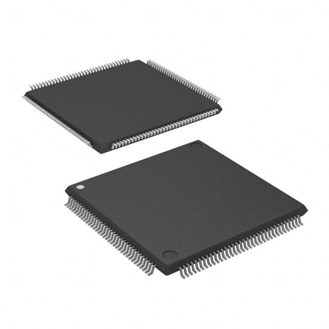
The device is available in a 144-LQFP package and is designed for surface mounting. It operates within an ambient temperature range of 0°C to 85°C (TJ). The MachXO family is known for its high I/O to logic density and lead-free/RoHS compliant packaging.
Key features include embedded and distributed memory, sysCLOCK PLLs for clock management, and compliance with IEEE 1149.1 Boundary Scan. The device is suitable for various embedded system applications requiring flexible logic implementation and control.
The LCMXO1200E-5TN144C FPGA features 1200 logic elements, 150 LABs, 9421 bits of total RAM, and 113 I/O pins. It operates within a voltage range of 1.14V to 1.26V.
The LCMXO1200E-5TN144C FPGA is available in a 144-LQFP package and is designed for surface mounting.
The operating temperature range for the LCMXO1200E-5TN144C FPGA is 0°C to 85°C (TJ).
Yes, the LCMXO1200E-5TN144C FPGA is RoHS3 Compliant.
The Moisture Sensitivity Level (MSL) for the LCMXO1200E-5TN144C FPGA is 1 Unlimited.