

| Distributor | Stock | Pricing | MOQ | PKG | Lead Time | Date Code | On Order Quantity | On Order Delivery | |
|---|---|---|---|---|---|---|---|---|---|
|
1,500 pcs
|
1500 pcs | On Request | 1 | On Request | On Request | On Request | On Request | On Request |
| Category | |
| Manufacturer Name | |
| Lead Spacing | |
| Mounting Type | |
| Number of I | |
| Number of LABs | |
| Number of Logic Elements | |
| Operating Temperature | |
| Supplier Device Package | |
| Supplier Package | |
| Tape & Reel | |
| Total RAM Bits | |
| Voltage |
The Lattice Semiconductor LCMXO1200E-3FTN256C is an FPGA from the MachXO family, designed for applications requiring glue logic, bus bridging, and control functions. This device features 1200 LUTs (Look-Up Tables) and 211 I/O pins, offering a high density of logic implementation.
Key electrical specifications include 9.2 kbits of Embedded Block RAM (EBR) and 6.4 kbits of Distributed RAM. The operating supply voltage ranges from 1.14V to 1.26V, with a nominal voltage of 1.2V. It supports a maximum operating frequency of 500 MHz and operates within a temperature range of 0°C to 85°C.
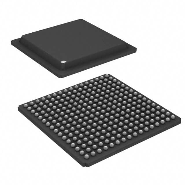
The device is packaged in a 256-FTBGA (17x17 mm) format and utilizes surface mount technology. It is designed for efficient in-system programming and offers features like instant-on capability and robust design security, characteristic of non-volatile FPGAs.
This FPGA is suitable for various embedded system designs where flexible logic implementation and reliable performance are critical. Its specifications make it a strong candidate for applications traditionally handled by CPLDs and low-capacity FPGAs.
The LCMXO1200E-3FTN256C has 1200 logic elements.
The LCMXO1200E-3FTN256C offers 211 I/O pins.
The operating supply voltage for the LCMXO1200E-3FTN256C is 1.2V.
The LCMXO1200E-3FTN256C is supplied in a 256-FTBGA package.
The maximum operating temperature for the LCMXO1200E-3FTN256C is 85°C.
The maximum operating frequency is 500 MHz.