

| Distributor | Stock | Pricing | MOQ | PKG | Lead Time | Date Code | On Order Quantity | On Order Delivery | |
|---|---|---|---|---|---|---|---|---|---|
|
5,716 pcs
|
5716 pcs | On Request | 1 | On Request | On Request | On Request | On Request | On Request |
| Category | |
| Manufacturer Name | |
| Lead Spacing | |
| Mounting Type | |
| Number of I | |
| Number of LABs | |
| Number of Logic Elements | |
| Operating Temperature | |
| Supplier Device Package | |
| Supplier Package | |
| Total RAM Bits | |
| Voltage |
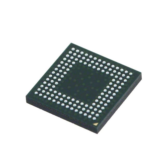
The Lattice Semiconductor LCMXO1200C-4MN132C is a Field Programmable Gate Array (FPGA) designed for applications requiring flexible logic implementation. This device offers 1200 logic elements and 150 LABs, providing substantial capacity for complex designs. It includes 9421 total RAM bits for embedded memory functions.
The FPGA features 101 I/O pins, supporting a wide range of interface requirements. It operates within a voltage range of 1.71V to 3.465V and has an operating temperature range of 0°C to 85°C (TJ). The device is housed in a 132-LFBGA, CSPBGA package and is designed for surface mounting.
This FPGA is part of the MachXO family, known for its non-volatile, infinitely reconfigurable architecture. It offers instant-on capability and excellent design security. The device is suitable for glue logic, bus bridging, and control logic applications.
The LCMXO1200C-4MN132C FPGA has 1200 logic elements.
The operating voltage range for this FPGA is 1.71V to 3.465V.
The LCMXO1200C-4MN132C offers 101 I/O pins.
The package type is 132-LFBGA, CSPBGA.
The operating temperature range is 0°C to 85°C (TJ).
This FPGA has a total of 9421 RAM bits.