

| Distributor | Stock | Pricing | MOQ | PKG | Lead Time | Date Code | On Order Quantity | On Order Delivery | |
|---|---|---|---|---|---|---|---|---|---|
|
1,259 pcs
|
1259 pcs | On Request | 1 | On Request | On Request | On Request | On Request | On Request | |
|
107 pcs
|
107 pcs | On Request | 1 | On Request | On Request | 11+ | On Request | On Request | |
|
6 pcs
|
6 pcs | On Request | 1 | On Request | On Request | On Request | On Request | On Request | |
|
1 pcs
|
1 pcs | On Request | 1 | On Request | On Request | On Request | On Request | On Request | |
|
1 pcs
|
1 pcs | On Request | 1 | On Request | On Request | On Request | On Request | On Request |
| Category | |
| Manufacturer Name | |
| AEC Qualified | |
| Automotive Grade | |
| Industrial Grade | |
| Lead Spacing | |
| Medical Grade | |
| Military Grade | |
| Mounting Type | |
| Number of I | |
| Number of I/O | |
| Number of LABs | |
| Number of Logic Elements | |
| Operating Temperature | |
| Operating Voltage | |
| Supplier Device Package | |
| Supplier Package | |
| Tape & Reel | |
| Total RAM Bits | |
| Voltage |
The Lattice Semiconductor LCMXO1200C-4FTN256C is a Field Programmable Gate Array (FPGA) designed for applications requiring flexible logic implementation. It features 1200 logic elements and 150 Logic Array Blocks (LABs), providing substantial processing capability.
This FPGA offers 211 input/output (I/O) pins and 9421 total RAM bits, supporting complex digital designs. It operates with a supply voltage ranging from 1.71V to 3.465V and has an operating temperature range of 0°C to 85°C (TJ).
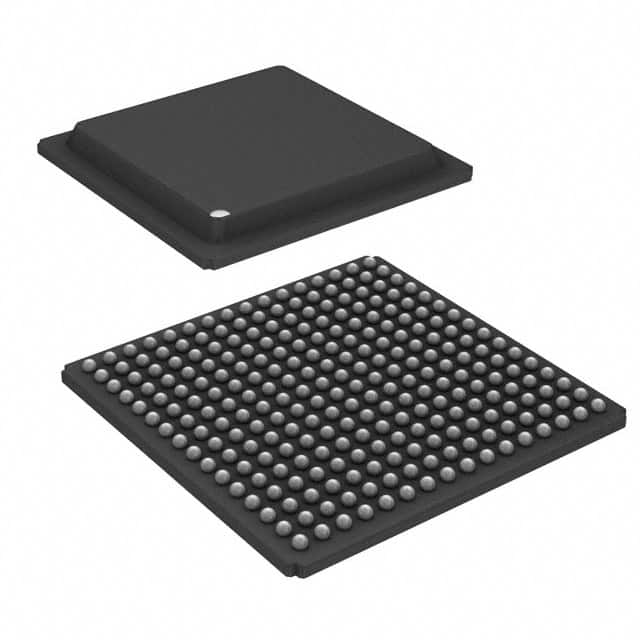
The device is housed in a 256-FTBGA (17x17) package, suitable for surface mount applications. It is also available in a 256-LBGA package. The LCMXO1200C-4FTN256C is part of the MachXO family, known for its non-volatile, infinitely reconfigurable architecture with instant-on capabilities.
Key features include support for various I/O interfaces such as LVCMOS, LVTTL, PCI, LVDS, Bus-LVDS, LVPECL, and RSDS. It also incorporates sysCLOCK PLLs for clock management and adheres to IEEE 1149.1 Boundary Scan standards.
The LCMXO1200C-4FTN256C FPGA has 1200 logic elements.
The LCMXO1200C-4FTN256C FPGA features 211 I/O pins.
The LCMXO1200C-4FTN256C FPGA operates within a voltage range of 1.71V to 3.465V.
The LCMXO1200C-4FTN256C FPGA is supplied in a 256-FTBGA (17x17) package and a 256-LBGA package.
The LCMXO1200C-4FTN256C FPGA has an operating temperature range of 0°C to 85°C (TJ).