

| Distributor | Stock | Pricing | MOQ | PKG | Lead Time | Date Code | On Order Quantity | On Order Delivery | |
|---|---|---|---|---|---|---|---|---|---|
|
2,660 pcs
|
2660 pcs | On Request | 1 | On Request | On Request | On Request | On Request | On Request | |
|
70 pcs
|
70 pcs | On Request | 1 | On Request | On Request | On Request | On Request | On Request |
| Category | |
| Manufacturer Name | |
| Current | |
| DC Current Gain (hFE) (Min) @ Ic, Vce | |
| Mounting Type | |
| Operating Temperature | |
| Power | |
| Supplier Device Package | |
| Transistor Type | |
| Turn Off Time | |
| Turn On Time | |
| Vce Saturation (Max) @ Ib, Ic | |
| Voltage |
The JANTX2N5665 is a high-performance NPN power silicon switching transistor manufactured by Microchip Technology. It is qualified per MIL-PRF-19500/455, indicating robust reliability for demanding applications.
This transistor features a maximum collector-emitter voltage of 300Vdc and a continuous collector current rating of 5Adc. Its absolute maximum power dissipation is rated at 2.5W at 25°C ambient temperature and 15W at 100°C case temperature. The operating and storage junction temperature range is from -65°C to +200°C.
Key electrical characteristics include a minimum DC current gain (hFE) of 25 at 1A collector current and 5V Vce, and a maximum collector-emitter saturation voltage of 1V at 5A collector current and 1A base current. The output capacitance is 120pF, and switching times are specified with a turn-on time of 0.25μs and a turn-off time of 2μs.
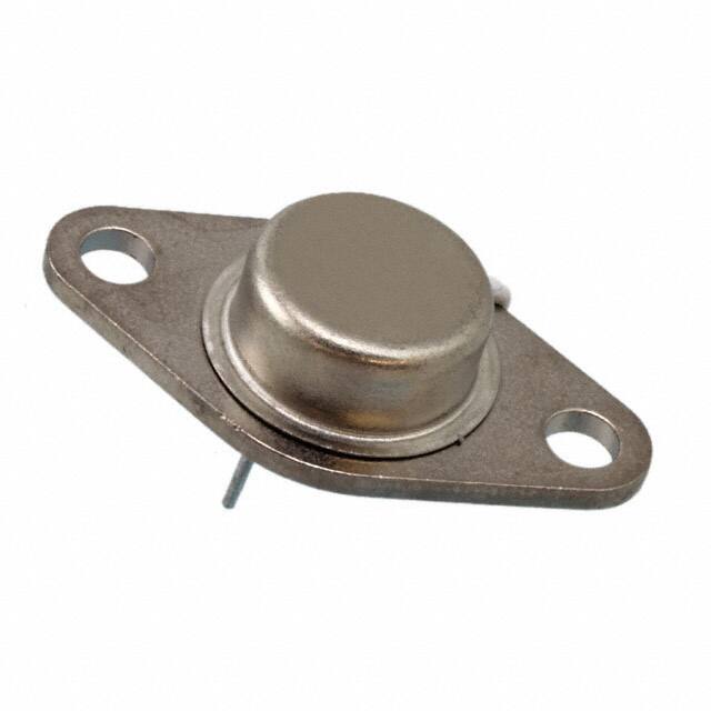
The JANTX2N5665 is supplied in a TO-66 (TO-213AA) package suitable for through-hole mounting. This makes it suitable for various power switching and amplification circuits where high voltage and current handling capabilities are required.
| Qty | Low | High |
|---|---|---|
| 1+ | $0.99 | $0.99 |
Estimated market price range - modelled values for guidance only, not live distributor offers.
The maximum collector-emitter voltage for the JANTX2N5665 is 300 Vdc.
The JANTX2N5665 has a continuous collector current rating of 5 Adc.
The operating and storage junction temperature range for the JANTX2N5665 is -65°C to +200°C.
The JANTX2N5665 is supplied in a TO-66 (TO-213AA) package.
The minimum DC current gain (hFE) for the JANTX2N5665 at 1A collector current and 5V Vce is 25.
The maximum turn-off time for the JANTX2N5665 is 2 μs.