

| Distributor | Stock | Pricing | MOQ | PKG | Lead Time | Date Code | On Order Quantity | On Order Delivery | |
|---|---|---|---|---|---|---|---|---|---|
|
1,900 pcs
|
1900 pcs | On Request | 1 | On Request | On Request | On Request | On Request | On Request | |
|
689 pcs
|
689 pcs | On Request | 1 | On Request | On Request | 1321+ | On Request | On Request |
| Category | |
| Manufacturer Name | |
| AEC Qualified | |
| Automotive Grade | |
| Differential | |
| Divider | |
| Frequency | |
| Industrial Grade | |
| Input | |
| Medical Grade | |
| Military Grade | |
| Mounting Type | |
| Number of Circuits | |
| Operating Temperature | |
| Operating Voltage | |
| Output | |
| PLL | |
| Programmable | |
| Ratio | |
| Supplier Device Package | |
| Type | |
| Voltage |
The Lattice Semiconductor ISPPAC-CLK5308S-01TN48I is an in-system-programmable zero-delay universal fan-out buffer designed for clock distribution applications. It supports input/output frequencies from 8MHz to 267MHz, featuring low output-to-output skew of less than 100ps and peak-to-peak jitter below 70ps.
This device offers up to 20 programmable fan-out buffers with support for various single-ended output standards including LVTTL, LVCMOS, HSTL, eHSTL, and SSTL. It provides programmable output impedance from 40 to 70 Ohms in 5 Ohm increments and programmable slew rate. The device supports up to 10 banks with individual VCCO and GND, operating at 1.5V, 1.8V, 2.5V, or 3.3V.
It features a fully integrated high-performance PLL with programmable lock detect, three "Power of 2" output dividers, and a programmable on-chip loop filter. The device is compatible with spread spectrum clocks and supports internal/external feedback. Precision programmable phase adjustment per output is available with 8 settings and a minimum step size of 156ps, offering up to +/- 5ns skew range.
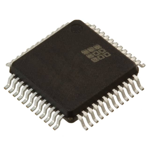
The ISPPAC-CLK5308S-01TN48I is housed in a 48-pin TQFP package and is suitable for circuit board common clock distribution, PLL-based frequency generation, and high fan-out clock buffering applications. It is hot-socket compliant and supports full JTAG boundary scan test in-system programming.
The input/output operation frequency ranges from 8MHz to 267MHz.
The output-to-output skew is less than 100 ps.
The peak-to-peak jitter is less than 70 ps.
Supported output standards include eHSTL, HSTL, LVCMOS, LVTTL, and SSTL.
The operating temperature range is -40°C to +85°C.
The device is available in a 48-TQFP (7x7) package.
The operating supply voltage is between 3V and 3.6V.