

| Distributor | Stock | Pricing | MOQ | PKG | Lead Time | Date Code | On Order Quantity | On Order Delivery | |
|---|---|---|---|---|---|---|---|---|---|
|
3,043 pcs
|
3043 pcs | On Request | 1 | On Request | On Request | 1725+ | On Request | On Request |
| Category | |
| Manufacturer Name | |
| Access Time | |
| Clock Frequency | |
| Data Rate | |
| Memory Format | |
| Memory Interface | |
| Memory Organization | |
| Memory Size | |
| Memory Type | |
| Mounting Type | |
| Operating Temperature | |
| SVHC Present | |
| Supplier Device Package | |
| Technology | |
| Voltage | |
| Write Cycle Time |
The IS46LR32160B-6BLA2 is a 512Mbit CMOS Mobile Double Data Rate Synchronous DRAM organized as 4 banks. This device utilizes a double-data-rate architecture for high-speed operation, with data input/output signals on a 32-bit bus. It supports a maximum clock frequency of 166 MHz and a maximum data rate of 333 Mbps/pin.
Key features include a JEDEC standard 1.8V power supply, LVCMOS compatible inputs/outputs, and support for various power-saving modes. The memory organization is 16M x 32, with configurable CAS latency (2 or 3) and burst length (2, 4, 8, 16). The component operates within a temperature range of -40°C to 105°C (TA).
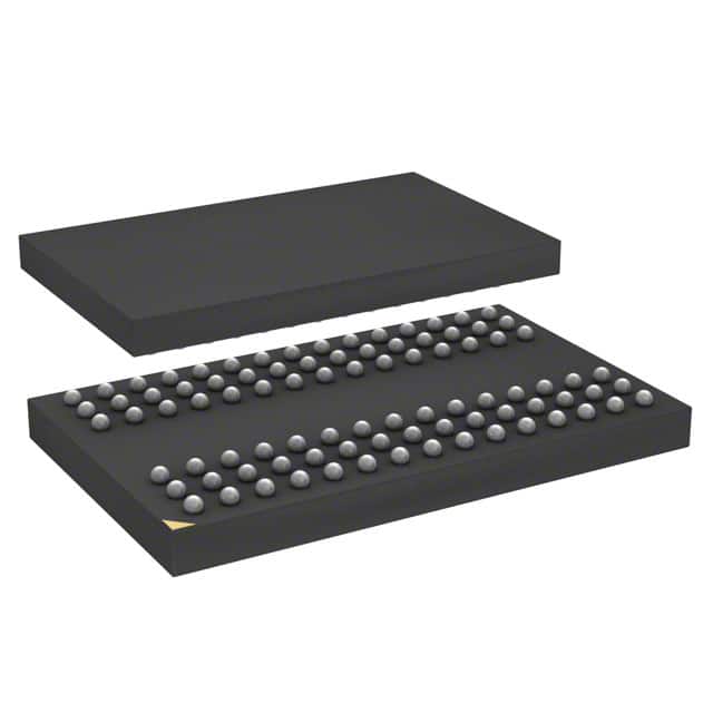
Packaged in a 90-TFBGA (8x13) format, the IS46LR32160B-6BLA2 is designed for surface mounting. It offers features like auto and self-refresh, concurrent auto precharge, and programmable driver strength control.
| Qty | Low | High |
|---|---|---|
| 1+ | $1.28 | $1.28 |
Estimated market price range - modelled values for guidance only, not live distributor offers.
The operating voltage is 1.8V for both VDD and VDDQ.
It is available in a 90-TFBGA (8x13mm) surface mount package.
The operating temperature range is -40°C to 105°C (TA).
The memory size is 512 Mbit, organized as 16M x 32.
The maximum clock frequency is 166 MHz.
It supports PASR, Auto TCSR, Deep Power Down Mode, and programmable driver strength control.
CAS latency of 2 and 3 are supported.