

| Distributor | Stock | Pricing | MOQ | PKG | Lead Time | Date Code | On Order Quantity | On Order Delivery | |
|---|---|---|---|---|---|---|---|---|---|
|
1,804 pcs
|
1804 pcs | On Request | 1 | On Request | On Request | On Request | On Request | On Request |
| Category | |
| Manufacturer Name | |
| Current | |
| Drain to Source Voltage (Vdss) | |
| Drive Voltage (Max Rds On, Min Rds On) | |
| FET Type | |
| Gate Charge (Qg) (Max) @ Vgs | |
| Halogen Free | |
| Industrial Grade | |
| Input Capacitance (Ciss) (Max) @ Vds | |
| Mounting Type | |
| Operating Temperature | |
| Power Dissipation (Max) | |
| Rds On (Max) @ Id, Vgs | |
| SVHC Present | |
| Storage Temperature | |
| Supplier Device Package | |
| Tape & Reel | |
| Technology | |
| Vgs (Max) | |
| Vgs(th) (Max) @ Id |
The IRLHM630TRPBF is a HEXFET power MOSFET from Infineon Technologies, featuring N-Channel enhancement mode technology. It is rated for a drain-source voltage of 30V and can deliver a continuous drain current of 40A at case temperature 25°C (21A at ambient). The device offers a low maximum on-resistance of 3.5mΩ at Vgs=4.5V and a typical on-resistance of 2.2mΩ at Vgs=10V, minimizing conduction losses. With a gate threshold voltage of 1.1V max, it is suitable for low-voltage gate drive applications. The total gate charge is 62nC max at 4.5V, enabling efficient switching.
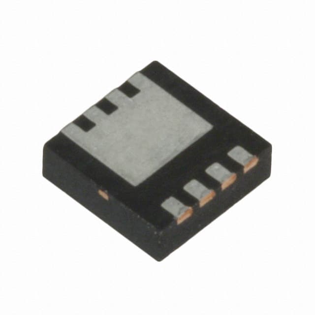
This MOSFET is housed in a compact 8-VQFN exposed pad package (PQFN 3.3x3.3mm) for surface mount assembly, offering low thermal resistance to the PCB (3.4°C/W). It is designed for applications such as battery-operated DC motor inverters and secondary side synchronous rectification. The device is RoHS compliant, MSL1, and contains no lead, bromine, or halogen according to the datasheet.
Key electrical characteristics include input capacitance of 3170pF typical at 25V, and pulsed drain current capability of 160A. The junction temperature range is -55°C to 150°C, with power dissipation of 2.7W at ambient and 37W at case temperature.
| Qty | Low | High |
|---|---|---|
| 1+ | $1.69 | $1.69 |
| 10+ | $1.07 | $1.07 |
Estimated market price range - modelled values for guidance only, not live distributor offers.
The drain-to-source voltage (Vdss) is 30V.
It is available in an 8-VQFN exposed pad package, also known as PQFN (3.3x3.3mm).
The junction temperature range is -55°C to 150°C.
Yes, it is marked as RoHS compliant in the datasheet and listed as RoHS3 compliant in the database, though that status is unverified.
The typical on-resistance is 2.2mΩ at Vgs=10V, Id=20A.
The maximum gate threshold voltage is 1.1V at Id=50µA.
The total gate charge is 62nC maximum at Vgs=4.5V, Vds=15V, Id=20A.