

| Distributor | Stock | Pricing | MOQ | PKG | Lead Time | Date Code | On Order Quantity | On Order Delivery | |
|---|---|---|---|---|---|---|---|---|---|
|
61,020 pcs
|
61020 pcs | On Request | 1 | On Request | On Request | On Request | On Request | On Request |
| Category | |
| Manufacturer Name | |
| Current | |
| Drain to Source Voltage (Vdss) | |
| Drive Voltage (Max Rds On, Min Rds On) | |
| FET Type | |
| Gate Charge (Qg) (Max) @ Vgs | |
| Halogen Free | |
| Input Capacitance (Ciss) (Max) @ Vds | |
| Mounting Type | |
| Operating Temperature | |
| Power Dissipation (Max) | |
| Rds On (Max) @ Id, Vgs | |
| SVHC Present | |
| Supplier Device Package | |
| Technology | |
| Vgs (Max) | |
| Vgs(th) (Max) @ Id |
The IRFSL7437PBF is an N-channel power MOSFET from Infineon Technologies, part of the HEXFET family. It features a drain-source voltage (Vdss) of 40V and a continuous drain current of 195A (package limited). The device offers a typical on-resistance of 1.4mΩ and a maximum of 1.8mΩ at Vgs=10V, enabling high efficiency in power conversion. The total gate charge is 225nC at 10V, and input capacitance is 7330pF at 25V.
This MOSFET is designed for high-current switching applications such as brushed and BLDC motor drives, synchronous rectification, DC/DC converters, AC/DC converters, DC/AC inverters, half-bridge and full-bridge topologies, and OR-ing or redundant power switches. It can dissipate up to 230W and operates over a junction temperature range of -55°C to 175°C.
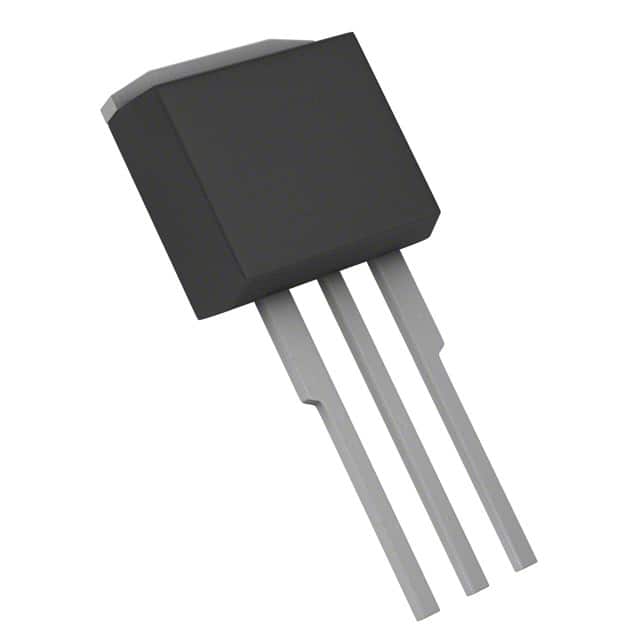
The device is supplied in a through-hole TO-262 package (also known as TO-262AA or I²Pak) with long leads. It is lead-free and halogen-free, and RoHS3 compliant (unverified). The standard packaging is a tube of 50 units.
The maximum drain-to-source voltage (Vdss) is 40 V.
The TO-262-3 Long Leads, I²Pak, TO-262AA package.
The junction temperature range is -55°C to 175°C.
RoHS3 compliant status is unverified low confidence; however, it is confirmed lead-free and halogen-free from the datasheet.
The maximum continuous drain current is 195A (package limited); silicon limit is 250A.
Typical on-resistance is 1.4mΩ, maximum 1.8mΩ at 100A and 10V gate-to-source voltage.
The maximum total gate charge is 225 nC at 10V gate-to-source voltage.