

| Distributor | Stock | Pricing | MOQ | PKG | Lead Time | Date Code | On Order Quantity | On Order Delivery | |
|---|---|---|---|---|---|---|---|---|---|
|
5,020 pcs
|
5020 pcs | On Request | 1 | On Request | On Request | On Request | On Request | On Request |
| Category | |
| Manufacturer Name | |
| Current | |
| Drain to Source Voltage (Vdss) | |
| Drive Voltage (Max Rds On, Min Rds On) | |
| FET Type | |
| Gate Charge (Qg) (Max) @ Vgs | |
| Input Capacitance (Ciss) (Max) @ Vds | |
| Mounting Type | |
| Operating Temperature | |
| Power Dissipation (Max) | |
| Rds On (Max) @ Id, Vgs | |
| Storage Temperature | |
| Supplier Device Package | |
| Technology | |
| Vgs (Max) | |
| Vgs(th) (Max) @ Id |
The IRFSL5615PBF is an N-Channel power MOSFET manufactured by Infineon Technologies. It is designed for high-performance applications, particularly Class-D audio amplifiers, where efficiency and signal fidelity are critical.
Key electrical specifications include a maximum drain-source voltage of 150V, continuous drain current of 33A at 25°C case temperature, and a maximum on-resistance of 42mOhm at 21A and 10V gate drive. The gate charge is 26nC typical (40nC max), and the switching gate charge (Qsw) is 11nC typical. Input capacitance is 1750pF at 50V drain-source voltage. Internal gate resistance is 2.7 Ohm typical.
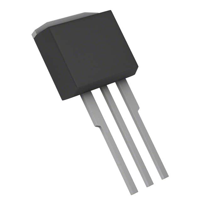
The device can dissipate up to 144W at 25°C case temperature and operates over a junction temperature range of -55°C to 175°C. Thermal resistance from junction to case is 1.045°C/W maximum. It is supplied in a through-hole TO-262-3 package (also compatible with I²Pak and TO-262AA).
This MOSFET is optimized for Class-D audio amplifier power stages, offering low RDS(on) and low gate charge for improved efficiency and total harmonic distortion. Compliance status is reported as RoHS3 compliant, REACH unaffected, and MSL 1 (unlimited), though these values are low-confidence and unverified.
150V maximum.
TO-262-3 Long Leads, I²Pak, TO-262AA (through-hole).
-55°C to 175°C junction temperature.
Reported as RoHS3 Compliant but unverified.
33A at 25°C case temperature, 10V gate drive.
34.5mOhm typical, 42mOhm maximum at 21A, 10V gate drive.
26nC typical, 40nC maximum at 10V gate drive.