

| Distributor | Stock | Pricing | MOQ | PKG | Lead Time | Date Code | On Order Quantity | On Order Delivery | |
|---|---|---|---|---|---|---|---|---|---|
|
11,020 pcs
|
11020 pcs | On Request | 1 | On Request | On Request | On Request | On Request | On Request |
| Category | |
| Manufacturer Name | |
| Current | |
| Drain to Source Voltage (Vdss) | |
| Drive Voltage (Max Rds On, Min Rds On) | |
| FET Type | |
| Gate Charge (Qg) (Max) @ Vgs | |
| Input Capacitance (Ciss) (Max) @ Vds | |
| Lead Style | |
| Mounting Type | |
| Operating Temperature | |
| Power Dissipation (Max) | |
| Rds On (Max) @ Id, Vgs | |
| Reverse Recovery Time | |
| SVHC Present | |
| Supplier Device Package | |
| Tape & Reel | |
| Technology | |
| Termination Style | |
| Vgs (Max) | |
| Vgs(th) (Max) @ Id |
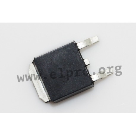
The IRFR3411TRPBF is an N-channel power MOSFET manufactured by Infineon Technologies (formerly International Rectifier). It is part of the HEXFET series, utilizing advanced process technology to achieve low on-resistance per silicon area. This device is rated for a maximum drain-source voltage of 100V and a continuous drain current of 32A at 25°C case temperature (23A at 100°C). The typical on-resistance is 44mOhm at 16A and 10V gate drive. The gate threshold voltage is 4V maximum at 250µA drain current. Total gate charge is 71nC at 10V, and input capacitance is 1960pF at 25V drain-source voltage. The device supports pulsed drain current up to 110A and is avalanche rated at 16A with repetitive avalanche energy of 13mJ. The body diode has a forward voltage of 1.2V and reverse recovery time of 115ns typical (170ns max). The MOSFET is housed in a surface-mount D-Pak package (TO-252-3, DPak, SC-63) with gull wing leads and two leads plus tab. It is designed for surface mounting using vapor phase, infrared, or wave soldering. Maximum power dissipation is 130W at 25°C case temperature with a linear derating factor of 0.83W/°C. Junction-to-case thermal resistance is 1.2°C/W, and junction-to-ambient is 50°C/W (PCB mount) or 110°C/W. The operating junction temperature range is -55°C to 175°C. This MOSFET is suitable for high-efficiency power conversion applications such as switch-mode power supplies, DC-DC converters, and motor control circuits.
The maximum drain-source voltage (Vdss) is 100V.
It is available in a surface mount D-Pak package (TO-252-3, DPak, SC-63).
The operating junction temperature range is -55°C to 175°C.
The datasheet indicates the part is lead-free, and it is listed as RoHS3 compliant, but this status is unverified.
The total gate charge is 71nC at 10V gate-source voltage.