

| Distributor | Stock | Pricing | MOQ | PKG | Lead Time | Date Code | On Order Quantity | On Order Delivery | |
|---|---|---|---|---|---|---|---|---|---|
|
11,100 pcs
|
11100 pcs | On Request | 1 | On Request | On Request | 17+ | On Request | On Request |
| Category | |
| Manufacturer Name | |
| Current | |
| Drain to Source Voltage (Vdss) | |
| Drive Voltage (Max Rds On, Min Rds On) | |
| FET Type | |
| Gate Charge (Qg) (Max) @ Vgs | |
| Halogen Free | |
| Input Capacitance (Ciss) (Max) @ Vds | |
| Lead Style | |
| Mounting Type | |
| Operating Temperature | |
| Power Dissipation (Max) | |
| Rds On (Max) @ Id, Vgs | |
| Storage Temperature | |
| Supplier Device Package | |
| Tape & Reel | |
| Technology | |
| Vgs (Max) | |
| Vgs(th) (Max) @ Id |
The Infineon IRFB7440GPBF is an N-Channel enhancement mode power MOSFET utilizing HEXFET technology. It is designed for high-current switching applications requiring low on-state resistance. The device is rated for a maximum drain-source voltage of 40V and a continuous drain current of 120A (package limited) at 25°C case temperature. The maximum on-resistance is 2.5mΩ at Vgs=10V and Id=100A, with a typical value of 2.0mΩ.
This MOSFET features a maximum gate threshold voltage of 3.9V at Id=100µA and a maximum gate charge of 135nC at Vgs=10V. The input capacitance is 4730pF at Vds=25V. The device is capable of handling pulsed drain currents up to 772A. The maximum power dissipation is 208W at Tc=25°C with a linear derating factor of 1.4 W/°C.
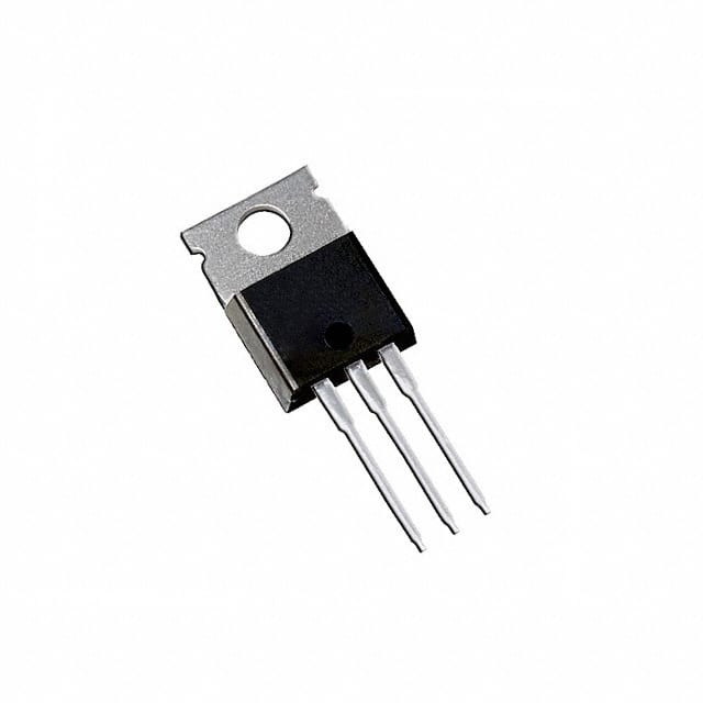
The IRFB7440GPBF is supplied in a standard TO-220AB through-hole package, suitable for PCB mounting. The device is lead-free and halogen-free per the datasheet. Typical applications include brushed and brushless DC motor drives, battery powered circuits, half-bridge and full-bridge topologies, synchronous rectification, resonant mode power supplies, OR-ing and redundant power switches, DC/DC and AC/DC converters, and DC/AC inverters.
| Qty | Low | High |
|---|---|---|
| 279+ | $1.08 | $1.08 |
Estimated market price range - modelled values for guidance only, not live distributor offers.
The maximum drain-source voltage (Vdss) is 40V.
The continuous drain current is 120A when limited by the package at Tc=25°C. The silicon die can handle 208A at Tc=25°C.
The maximum on-resistance is 2.5mΩ at Vgs=10V and Id=100A. Typical on-resistance is 2.0mΩ.
The device is supplied in a TO-220AB through-hole package.
The operating junction temperature range is -55°C to 175°C.
The datasheet indicates the device is lead-free and halogen-free. RoHS compliance status is unverified in the source data.