

Have a small number of parts or want to add parts manually? Request Quote manually

Search across all market segments

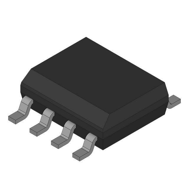
IRF8313PBF The IRF8313PBF is a dual N-channel power MOSFET from Infineon Technologies, rated for 30V drain-source voltage and 9.7A continuous drain current. It features low on-resistance and gate charge, making it suitable for high-efficiency DC-DC conversion.
Mfr Part #:

IRF8313PBF

Available from 1 distributors
Mfr Name: Infineon Technologies
Infineon Technologies
The IRF8313PBF is a dual N-channel power MOSFET from Infineon Technologies, rated for 30V drain-source voltage and 9.7A continuous drain current. It features low on-resistance and gate charge, making it suitable for high-efficiency DC-DC conversion.
Total Stock: 6,000 pcs

IRF8313PBF Available from 1 distributor

Authorised
Non-Authorised
Distributor Stock Pricing MOQ PKG Lead Time Date Code On Order Quantity On Order Delivery
Non-Authorised Inventory information
6,000 pcs
6000 pcs On Request 1 On Request On Request On Request On Request On Request

IRF8313PBF Specifications Quick View

Most important parameters for selection – full specs in datasheet.
Category
Manufacturer Name
Configuration
Continuous Drain Current (Maximum @ TA = +70 °C, VGS = 10 V)
Current
Drain Source Leakage Current (Maximum @ VDS=24 V, VGS=0 V, TJ=125 °C)
Drain Source Leakage Current (Maximum @ VDS=24 V, VGS=0 V, TJ=25 °C)
Drain Source On Resistance (Typical/Maximum @ VGS=10 V, ID=9.7 A)
Drain Source On Resistance (Typical/Maximum @ VGS=4.5 V, ID=8.0 A)
Drain to Source Voltage (Vdss)
Drain-to-source breakdown voltage
FET Feature
Forward Transconductance
Gate Charge (Qg) (Max) @ Vgs
Gate-to-Source Leakage Current
Gate-to-Source Voltage (Max)
Halogen Free
Input Capacitance (Ciss) (Max) @ Vds
Junction to Ambient Thermal Resistance
Junction-to-Drain Lead Thermal Resistance
Lead Style
Mounting Type
Operating Temperature
Power
Power Dissipation (Maximum @ TA=70 °C)
Pulsed Drain Current
Rds On (Max) @ Id, Vgs
Storage Temperature
Supplier Device Package
Technology
Total Gate Charge (Maximum @ VDS=15 V, VGS=10 V, ID=8.0 A)
Total Gate Charge (Typical/Maximum @ VDS=15 V, VGS=4.5 V, ID=8.0 A)
Vgs(th) (Max) @ Id

IRF8313PBF Description

Short technical summary and product information.

The IRF8313PBF is a dual N-channel power MOSFET from Infineon Technologies, part of the HEXFET family. It is designed for high-efficiency power conversion applications, featuring a maximum drain-source voltage of 30V and a continuous drain current of 9.7A at 25°C. The device offers a low maximum on-resistance of 15.5mΩ at VGS=10V, and a typical gate charge of 6.0nC at VGS=4.5V, which helps reduce both conduction and switching losses.


This MOSFET is optimized for synchronous buck converters and other DC-DC conversion circuits, where low Rds(on) and gate charge are critical for efficiency. The logic-level gate allows operation with 4.5V drive, and the device is fully characterized for avalanche voltage and current. The IRF8313PBF is housed in an industry-standard SO-8 package and is surface-mountable, suitable for compact PCB designs.


The device operates over a junction temperature range of -55°C to 175°C, with a maximum power dissipation of 2.0W at 25°C ambient. It is lead-free and RoHS compliant (halogen-free), meeting modern environmental requirements. The dual-channel configuration in a single package saves board space and simplifies layout in multi-phase or bridge applications.

IRF8313PBF Quick Information

Product Type: MOSFET Array
Series: HEXFET
Canonical Name: IRF8313PBF Dual N-Channel Power MOSFET
Subcategory: Dual N-Channel MOSFET Array

IRF8313PBF Compliance

RoHS Status: RoHS Compliant
Moisture Sensitivity Level (MSL): 1 Unlimited
REACH Status: REACH Unaffected
Lead Free: Yes

IRF8313PBF Features

  • Dual N-channel MOSFET in SO-8 package.
  • 30V drain-source voltage rating.
  • Low on-resistance of 15.5mΩ at 10V.
  • Logic-level gate drive capability.
  • RoHS compliant and halogen-free.

IRF8313PBF Applications

  • Ideal for synchronous buck converters.
  • Used in DC-DC conversion circuits.
  • Suitable for load switching applications.
  • Power management in portable devices.

IRF8313PBF FAQs

7 frequently asked questions generated from this part’s specifications.
What is the maximum drain-to-source voltage of the IRF8313PBF?

The maximum drain-to-source voltage is 30V.

What is the maximum continuous drain current at 25°C?

The maximum continuous drain current is 9.7A at TA=25°C with VGS=10V.

What is the on-resistance of the IRF8313PBF?

The maximum on-resistance is 15.5mΩ at VGS=10V and ID=9.7A, and 21.6mΩ at VGS=4.5V and ID=8.0A.

What is the operating temperature range?

The operating junction temperature range is -55°C to 175°C.

Is the IRF8313PBF RoHS compliant?

Yes, the IRF8313PBF is RoHS compliant and halogen-free, as stated in the datasheet.

What package is the IRF8313PBF available in?

The IRF8313PBF is available in an 8-SOIC (0.154", 3.90mm Width) package, also known as 8-SO.

What is the gate threshold voltage of the IRF8313PBF?

The gate threshold voltage ranges from 1.35V minimum to 2.35V maximum, with a typical value of 1.80V at ID=25µA.

Home
Categories
Submit RFQ
Login
Account

Categories