

| Distributor | Stock | Pricing | MOQ | PKG | Lead Time | Date Code | On Order Quantity | On Order Delivery | |
|---|---|---|---|---|---|---|---|---|---|
|
4,700 pcs
|
4700 pcs | On Request | 1 | On Request | On Request | On Request | On Request | On Request | |
|
1,070 pcs
|
1070 pcs | On Request | 1 | On Request | On Request | On Request | On Request | On Request | |
|
137 pcs
|
137 pcs | On Request | 1 | On Request | On Request | 1325+ | On Request | On Request |
| Category | |
| Manufacturer Name | |
| Current | |
| Drain to Source Voltage (Vdss) | |
| Drive Voltage (Max Rds On, Min Rds On) | |
| FET Type | |
| Gate Charge (Qg) (Max) @ Vgs | |
| Halogen Free | |
| Industrial Grade | |
| Input Capacitance (Ciss) (Max) @ Vds | |
| Mounting Type | |
| Operating Temperature | |
| Power Dissipation (Max) | |
| Rds On (Max) @ Id, Vgs | |
| Supplier Device Package | |
| Technology | |
| Vgs (Max) | |
| Vgs(th) (Max) @ Id |
The IPW65R019C7 is a 650V N-Channel enhancement mode power MOSFET from Infineon's CoolMOS C7 series, built on the superjunction (SJ) principle. This device is designed for high efficiency in hard switching applications such as power factor correction (PFC) stages and PWM converters.
Key electrical specifications include a maximum drain-source voltage of 650V (700V at maximum junction temperature), a continuous drain current of 75A, and a maximum on-resistance of just 19mΩ at 58.3A and 10V gate drive. The device features a typical gate charge of 215nC and an input capacitance of 9900pF at 400V drain-source voltage.
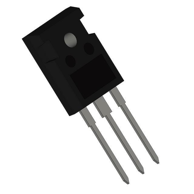
The IPW65R019C7 is housed in a standard TO-247-3 through-hole package (PG-TO247-3). It is qualified for industrial grade applications per JEDEC standards and features Pb-free plating and halogen-free mold compound.
The maximum drain-source voltage (Vdss) is 650V, with a maximum rating of 700V at maximum junction temperature.
The maximum continuous drain current is 75A at the case temperature (Tc).
The maximum drain-source on-resistance (Rds On) is 19mΩ at a drain current of 58.3A and a gate-source voltage of 10V.
It is available in a TO-247-3 through-hole package (PG-TO247-3).
The operating junction temperature range is -55°C to 150°C.
The datasheet states the device has Pb-free plating and halogen-free mold compound. The RoHS status in the database is unverified.
The typical gate charge (Qg) is 215nC at a gate-source voltage of 10V.