

| Distributor | Stock | Pricing | MOQ | PKG | Lead Time | Date Code | On Order Quantity | On Order Delivery | |
|---|---|---|---|---|---|---|---|---|---|
|
5,215 pcs
|
5215 pcs | On Request | 1 | On Request | On Request | 16+18 | On Request | On Request | |
|
1,803 pcs
|
1803 pcs | On Request | 1 | On Request | On Request | On Request | On Request | On Request | |
|
19 pcs
|
19 pcs | On Request | 1 | On Request | On Request | On Request | On Request | On Request |
| Category | |
| Manufacturer Name | |
| Gate Charge | |
| Halogen Free | |
| Mounting Type | |
| Package / Case |
The Infineon IPW60R190P6 is a high-voltage N-channel power MOSFET from the CoolMOS P6 series. Designed using the superjunction principle, this transistor offers significant advantages in power conversion efficiency.
Key electrical characteristics include a maximum Drain-Source Voltage (Vds) of 650V, a maximum On-Resistance (Rds(on)) of 190mΩ, and a typical Gate Charge (Qg) of 37nC. It also features a pulsed drain current (Id,pulse) of 57A and low energy in output capacitance (Eoss) of 4.9µJ at 400V.
This MOSFET is designed for applications such as PFC stages, hard-switching PWM stages, and resonant switching stages. Its features include increased dv/dt ruggedness, high commutation ruggedness, and ease of use. The device is Pb-free plated and halogen-free.
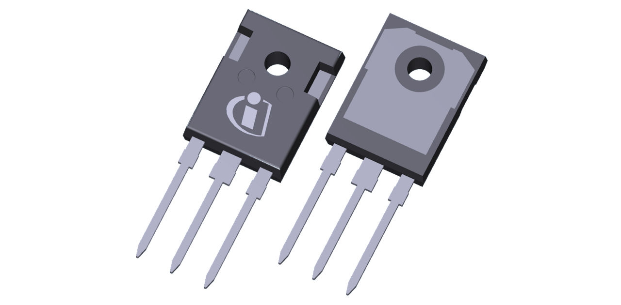
The IPW60R190P6 is supplied in a PG-TO 247 package, suitable for through-hole mounting. It is qualified for industrial-grade applications according to JEDEC standards.
The maximum Drain-Source Voltage (Vds) is 650V.
The maximum On-Resistance (Rds(on)) is 190mΩ.
The typical Gate Charge (Qg) is 37nC.
The IPW60R190P6 is supplied in a PG-TO 247 package.
The RoHS Status is RoHS3 Compliant.
The Moisture Sensitivity Level (MSL) is 1 Unlimited.
The REACH Status is REACH Unaffected.