
0402N680F500CG
Walsin Technology
The Walsin Technology 0402N680F500CG is a ceramic capacitor. It features RoHS3 compliance and MSL Level 1.


| Distributor | Stock | Pricing | MOQ | PKG | Lead Time | Date Code | On Order Quantity | On Order Delivery | |
|---|---|---|---|---|---|---|---|---|---|
|
720 pcs
|
720 pcs | On Request | 1 | On Request | On Request | On Request | On Request | On Request |
| Category | |
| Manufacturer Name | |
| AEC Qualified | |
| Automotive Grade | |
| Industrial Grade | |
| Medical Grade | |
| Military Grade | |
| Storage Temperature | |
| Tape & Reel |
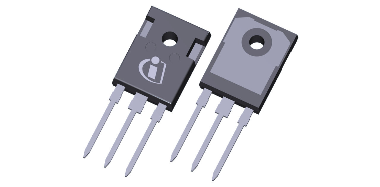
The Infineon Technologies IPW60R060P7 is a 600V N-channel Power MOSFET belonging to the CoolMOS P7 generation. This technology is designed for high-voltage power applications, offering a combination of efficiency and ease of use.
Key electrical specifications include a maximum Drain-Source Voltage (VDS) of 650V, a maximum On-Resistance (RDS(on)) of 60mΩ, and a typical Gate Charge (Qg) of 67nC. It also has a pulsed drain current (ID,pulse) of 151A and an output capacitance (Eoss) of 7.1µJ at 400V. The body diode exhibits a diF/dt rating of 900 A/µs.
This MOSFET is suitable for both hard and soft switching applications, including PFC and LLC stages, due to its commutation ruggedness and low ringing tendency. The design emphasizes reduced switching and conduction losses, contributing to more efficient, compact, and cooler system designs. It is fully qualified according to JEDEC for industrial applications.
The IPW60R060P7 is packaged in a PG-TO 247-3 through-hole configuration. Its features, such as excellent ESD robustness (>2kV HBM), enable increased power density solutions with smaller footprints and higher manufacturing quality.
| Qty | Low | High |
|---|---|---|
| 1+ | $0.99 | $0.99 |
Estimated market price range - modelled values for guidance only, not live distributor offers.
The maximum Drain-Source Voltage (VDS) at Tj,max is 650V.
The maximum On-Resistance (RDS(on)) is 60mΩ.
The typical Gate Charge (Qg) is 67nC.
The IPW60R060P7 is supplied in a PG-TO 247-3 package.
