

| Distributor | Stock | Pricing | MOQ | PKG | Lead Time | Date Code | On Order Quantity | On Order Delivery | |
|---|---|---|---|---|---|---|---|---|---|
|
2,200 pcs
|
2200 pcs | On Request | 1 | On Request | On Request | On Request | On Request | On Request | |
|
1,774 pcs
|
1774 pcs | On Request | 1 | On Request | On Request | On Request | On Request | On Request |
| Category | |
| Manufacturer Name | |
| Current | |
| Drain to Source Voltage (Vdss) | |
| Drive Voltage (Max Rds On, Min Rds On) | |
| FET Type | |
| Gate Charge (Qg) (Max) @ Vgs | |
| Input Capacitance (Ciss) (Max) @ Vds | |
| Mounting Type | |
| Operating Temperature | |
| Power Dissipation (Max) | |
| Rds On (Max) @ Id, Vgs | |
| Reverse Recovery Time | |
| SVHC Present | |
| Storage Temperature | |
| Supplier Device Package | |
| Technology | |
| Vgs (Max) | |
| Vgs(th) (Max) @ Id |
The IPP045N10N3G is a 100V N-Channel MOSFET manufactured by Infineon Technologies. It utilizes MOSFET (Metal Oxide) technology and is designed for high-frequency switching and synchronous rectification applications.
This device offers a continuous drain current of 137A at Tc=25°C and 105A at Tc=100°C, with a pulsed drain current capability of 548A. The drain-source on-state resistance is typically 3.9mΩ and maximum 4.5mΩ at Vgs=10V. Gate threshold voltage ranges from 2V to 3.5V. The MOSFET can handle a power dissipation of 214W at Tc=25°C and operates over a junction temperature range of -55°C to 175°C.
Switching characteristics include typical turn-on delay of 27ns, rise time of 59ns, turn-off delay of 48ns, and fall time of 14ns. Input capacitance is 6320pF to 8410pF, output capacitance 1210pF to 1610pF, and reverse transfer capacitance 41pF. Total gate charge is 88nC to 117nC.
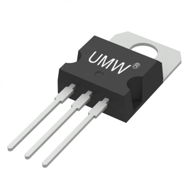
The device is available in a through-hole package (TO-220). It is RoHS compliant and has Pb-free lead plating. Thermal resistance from junction to case is 0.7 K/W, and junction to ambient is 62 K/W (minimal footprint) or 50 K/W (with 6 cm² cooling area).
-55°C to 175°C (junction temperature).
Yes, it is RoHS compliant.
137A continuous at Tc=25°C, 105A at Tc=100°C, and 548A pulsed.
4.5mΩ maximum at Vgs=10V, Id=100A.
2V typical, 3.5V maximum at Id=150µA.
214W maximum at Tc=25°C.