

| Distributor | Stock | Pricing | MOQ | PKG | Lead Time | Date Code | On Order Quantity | On Order Delivery | |
|---|---|---|---|---|---|---|---|---|---|
|
3,043 pcs
|
3043 pcs | On Request | 1 | On Request | On Request | On Request | On Request | On Request |
| Category | |
| Manufacturer Name | |
| Current | |
| Drain to Source Voltage (Vdss) | |
| Drive Voltage (Max Rds On, Min Rds On) | |
| FET Type | |
| Gate Charge (Qg) (Max) @ Vgs | |
| Halogen Free | |
| Industrial Grade | |
| Input Capacitance (Ciss) (Max) @ Vds | |
| Mounting Type | |
| Operating Temperature | |
| Power Dissipation (Max) | |
| Rds On (Max) @ Id, Vgs | |
| Supplier Device Package | |
| Tape & Reel | |
| Technology | |
| Termination Style | |
| Vgs (Max) | |
| Vgs(th) (Max) @ Id |
The IPL60R650P6SATMA1 is an N-Channel power MOSFET from Infineon Technologies, part of the CoolMOS P6 superjunction (SJ) series. It is designed for high efficiency in switching applications, featuring a maximum drain-source voltage of 650V at elevated junction temperature (nominal 600V) and a continuous drain current of 6.7A at case temperature. The on-resistance is rated at a maximum of 0.65Ω (650mΩ) with 10V gate drive. This MOSFET offers low gate charge (12nC typical) and input capacitance (557pF at 100V Vds), contributing to reduced switching losses. It also features a fast body diode with 500A/µs di/dt ruggedness and an output capacitance energy of 1.8µJ at 400V.
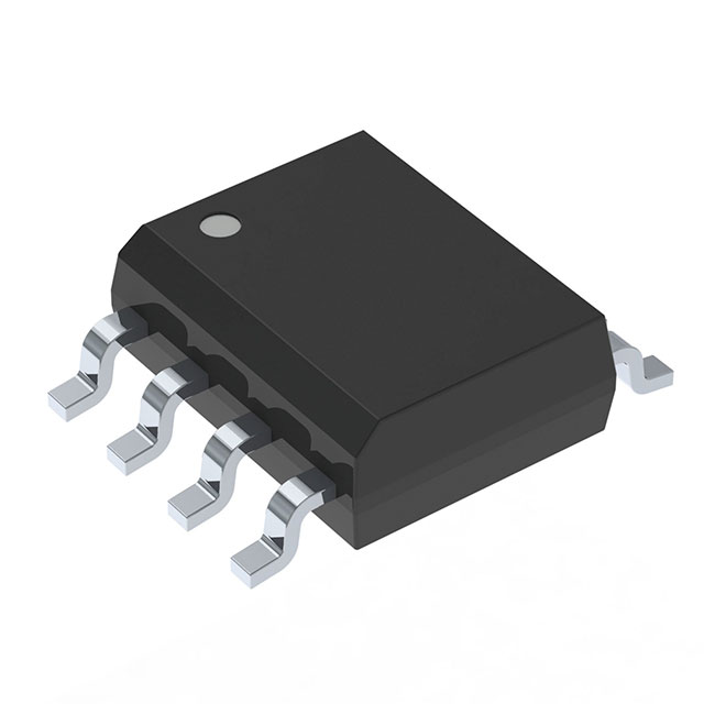
Key performance parameters include a pulsed drain current capability of 16.5A, a power dissipation of 56.8W, and an operating junction temperature range of -40°C to 150°C. The device is housed in a ThinPAK 5x6 (8-PowerTDFN) surface mount package with SMD gull wing terminations, compatible with standard assembly processes. The datasheet confirms Pb-free plating and halogen free mold compound, though formal RoHS and REACH compliance status remain unverified.
Applications include power factor correction (PFC) stages, hard switching and resonant switching PWM stages found in PC silverbox, adapters, LCD and PDP TVs, lighting, server, telecom, and UPS systems. The CoolMOS P6 technology provides extremely low figure of merit (FOM = Rdson*Qg) and Eoss, enabling compact, cool, and efficient power designs.
| Qty | Low | High |
|---|---|---|
| 1+ | $2.26 | $2.26 |
| 10+ | $1.43 | $1.43 |
| 100+ | $0.94 | $0.94 |
| 500+ | $0.74 | $0.74 |
| 1,000+ | $0.66 | $0.66 |
| 2,500+ | $0.60 | $0.60 |
| 5,000+ | $0.57 | $0.57 |
| 10,000+ | $0.56 | $0.56 |
Estimated market price range - modelled values for guidance only, not live distributor offers.
The maximum drain-source voltage is 650V at maximum junction temperature (Tj,max), with a nominal rating of 600V.
It comes in a ThinPAK 5x6 (8-PowerTDFN) surface mount package with SMD gull wing termination.
-40°C to 150°C (junction temperature).
The component has Pb-free plating and halogen free mold compound per the datasheet, but RoHS compliance status is unverified from the manufacturer.
Maximum on-resistance is 0.65Ω at Vgs=10V and Id=2.4A.
Typical gate charge is 12nC at Vgs=10V.
Designed for PFC stages, hard switching and resonant switching PWM stages in PC silverbox, adapter, TV, lighting, server, telecom, and UPS.