

| Distributor | Stock | Pricing | MOQ | PKG | Lead Time | Date Code | On Order Quantity | On Order Delivery | |
|---|---|---|---|---|---|---|---|---|---|
|
5,050 pcs
|
5050 pcs | On Request | 1 | On Request | On Request | On Request | On Request | On Request |
| Category | |
| Manufacturer Name | |
| AEC Qualified | |
| Automotive Grade | |
| Configuration | |
| Current | |
| Drain to Source Voltage (Vdss) | |
| FET Feature | |
| Gate Charge (Qg) (Max) @ Vgs | |
| Input Capacitance (Ciss) (Max) @ Vds | |
| Mounting Type | |
| Operating Temperature | |
| Power | |
| Rds On (Max) @ Id, Vgs | |
| Reverse Recovery Time | |
| Supplier Device Package | |
| Tape & Reel | |
| Technology | |
| Vgs(th) (Max) @ Id |
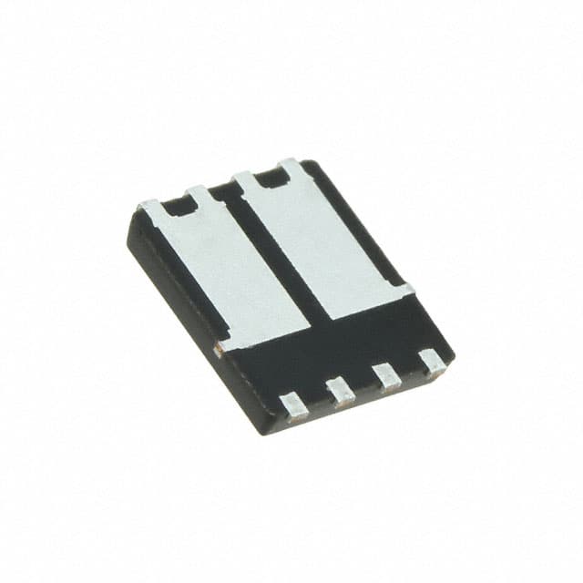
The IPG20N06S4L26ATMA1 is a dual N-channel enhancement mode Logic Level MOSFET from Infineon's OptiMOS-T2 family. It is qualified to AEC Q101 automotive standard and operates at junction temperatures up to 175°C. The device features a drain-source breakdown voltage of 60V and can handle a continuous drain current of 20A per channel at 25°C case temperature. The maximum on-state resistance is 26mOhm at VGS=10V and ID=17A, and 46mOhm at VGS=4.5V and ID=10A, enabling efficient switching at logic-level gate drives. Switching performance is characterized by a typical total gate charge of 20nC, input capacitance of 1430pF, and fast turn-on/off times. The MOSFET includes an integrated gate-to-source and gate-to-drain charge optimized for low switching losses. The body diode has a forward voltage of 1.3V maximum and a reverse recovery time of 33ns typical. The device is housed in a PG-TDSON-8 surface-mount package with a maximum junction-to-case thermal resistance of 4.5 K/W. It is MSL1 rated up to 260°C peak reflow and RoHS compliant.
| Qty | Low | High |
|---|---|---|
| 1+ | $2.04 | $2.04 |
| 10+ | $1.28 | $1.28 |
| 100+ | $0.75 | $0.75 |
| 500+ | $0.63 | $0.63 |
| 1,000+ | $0.54 | $0.54 |
| 5,000+ | $0.50 | $0.50 |
Estimated market price range - modelled values for guidance only, not live distributor offers.
The maximum drain-source voltage (Vds) is 60V.
The continuous drain current per channel is 20A at TC=25°C and 18A at TC=100°C, with VGS=10V.
The maximum on-resistance at VGS=10V and ID=17A is 26mOhm.
The gate threshold voltage (Vgs(th)) ranges from 1.2V minimum to 2.2V maximum, with a typical value of 1.7V.
The device is supplied in a PG-TDSON-8 surface-mount package (supplier device package PG-TDSON-8-4).
The operating junction temperature range is -55°C to 175°C.
Yes, the datasheet states it is a 'Green Product (RoHS compliant)'.