

| Distributor | Stock | Pricing | MOQ | PKG | Lead Time | Date Code | On Order Quantity | On Order Delivery | |
|---|---|---|---|---|---|---|---|---|---|
|
1,743 pcs
|
1743 pcs | On Request | 1 | On Request | On Request | On Request | On Request | On Request |
| Category | |
| Manufacturer Name | |
| Gate Charge | |
| Mounting Type | |
| Storage Temperature | |
| Tape & Reel |
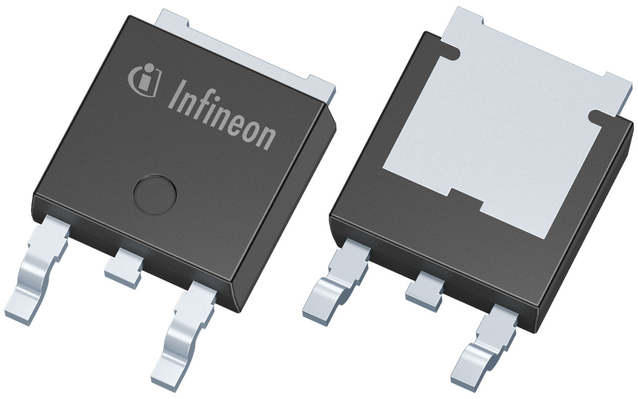
The Infineon Technologies IPD95R450P7 is a 950V N-channel Power MOSFET utilizing the advanced CoolMOS P7 super junction technology. This series sets new benchmarks in high-voltage MOSFET performance, combining efficiency with ease of use. It features best-in-class FOM (Figure of Merit) for RDS(on) * Eoss, reduced gate charge (Qg), and input/output capacitance (Ciss/Coss).
Key electrical characteristics include a maximum Drain-Source Voltage (VDS) of 950V, a maximum On-Resistance (RDS(on)) of 0.45Ω, and a typical Gate Charge (Qg) of 35nC. The typical Gate Threshold Voltage (VGS(th)) is 3V with a small variation of ±0.5V. It also includes integrated ESD protection via a Zener diode.
This device is supplied in a PG-TO252-3 package suitable for surface mounting. It is recommended for flyback topologies in applications such as LED lighting, low-power chargers and adapters, smart meters, and industrial power supplies. It is also suitable for PFC stages in consumer and solar applications. The product is fully qualified according to JEDEC standards for industrial applications.
| Qty | Low | High |
|---|---|---|
| 1+ | $0.99 | $0.99 |
Estimated market price range - modelled values for guidance only, not live distributor offers.
The maximum Drain-Source Voltage (VDS) at Tj=25°C is 950V.
The maximum On-Resistance (RDS(on)) is 0.45Ω.
The typical Gate Charge (Qg) is 35nC.
The IPD95R450P7 is supplied in a PG-TO252-3 package.
It is recommended for flyback topologies in LED lighting, low-power chargers and adapters, smart meters, AUX power, and industrial power supplies. It is also suitable for PFC stages in consumer and solar applications.