

| Distributor | Stock | Pricing | MOQ | PKG | Lead Time | Date Code | On Order Quantity | On Order Delivery | |
|---|---|---|---|---|---|---|---|---|---|
|
14,020 pcs
|
14020 pcs | On Request | 1 | On Request | On Request | On Request | On Request | On Request |
| Category | |
| Manufacturer Name | |
| Current | |
| Drain to Source Voltage (Vdss) | |
| Drive Voltage (Max Rds On, Min Rds On) | |
| FET Type | |
| Gate Charge (Qg) (Max) @ Vgs | |
| Halogen Free | |
| Industrial Grade | |
| Input Capacitance (Ciss) (Max) @ Vds | |
| Lead Style | |
| Mounting Type | |
| Operating Temperature | |
| Power Dissipation (Max) | |
| Rds On (Max) @ Id, Vgs | |
| Storage Temperature | |
| Supplier Device Package | |
| Tape & Reel | |
| Technology | |
| Termination Style | |
| Vgs (Max) | |
| Vgs(th) (Max) @ Id |
The IPB65R190C7ATMA2 is an N-Channel enhancement-mode power MOSFET from Infineon Technologies' CoolMOS C7 series. It utilizes superjunction (SJ) technology to achieve low on-resistance and fast switching performance. Key electrical specifications include a maximum drain-to-source voltage of 650V (700V breakdown at maximum junction temperature), a continuous drain current of 13A at Tc, and a pulsed drain current capability of 49A. The maximum on-resistance is 190mOhm at 10V gate drive, with a typical gate charge of 23nC and input capacitance of 1150pF at 400V. The device also features an output capacitance energy of 2.7µJ and a body diode di/dt of 55A/µs.
Designed for hard-switching topologies, this MOSFET is well-suited for power factor correction (PFC) stages and PWM stages in applications such as computing, server, telecom, UPS, and solar inverters. The CoolMOS C7 series offers improved efficiency through best-in-class figures of merit (RDS(on)*Eoss and RDS(on)*Qg) and increased dv/dt ruggedness.
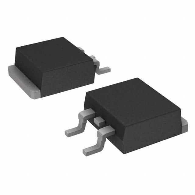
The device is housed in a surface-mount PG-TO263-3 (D²PAK) package with gull wing leads. It is Pb-free plated and uses a halogen-free mold compound, meeting industrial-grade qualification standards per JEDEC. The operating junction temperature range is -55°C to 150°C.
| Qty | Low | High |
|---|---|---|
| 1+ | $4.14 | $4.14 |
| 10+ | $2.72 | $2.72 |
| 100+ | $2.04 | $2.04 |
| 500+ | $1.71 | $1.71 |
| 1,000+ | $1.48 | $1.48 |
Estimated market price range - modelled values for guidance only, not live distributor offers.
The maximum drain-to-source voltage (Vdss) is 650V, with a breakdown voltage of 700V at maximum junction temperature.
The maximum continuous drain current is 13A at case temperature Tc.
It is offered in a surface-mount PG-TO263-3 (D²PAK) package with gull wing leads.
The operating junction temperature range is -55°C to 150°C.
The datasheet indicates Pb-free plating and halogen-free mold compound, and the part is listed as RoHS3 compliant.
The typical gate charge is 23nC at 10V gate drive.
The maximum on-resistance is 190mOhm at 5.7A drain current and 10V gate voltage.