

| Distributor | Stock | Pricing | MOQ | PKG | Lead Time | Date Code | On Order Quantity | On Order Delivery | |
|---|---|---|---|---|---|---|---|---|---|
|
55 pcs
|
55 pcs | On Request | 1 | On Request | On Request | On Request | On Request | On Request |
| Category | |
| Manufacturer Name | |
| AEC Qualified | |
| Automotive Grade | |
| Differential | |
| Frequency | |
| Industrial Grade | |
| Input | |
| Input Capacitance | |
| Medical Grade | |
| Military Grade | |
| Mounting Type | |
| Number of Circuits | |
| Operating Temperature | |
| Output | |
| Propagation Delay | |
| Ratio | |
| Supplier Device Package | |
| Tape & Reel | |
| Technology | |
| Type | |
| Voltage |
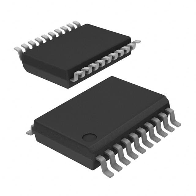
The Renesas IDT74FCT3807AQ is a 3.3V CMOS clock driver designed for efficient clock distribution. This device offers a 1:10 fanout ratio, allowing a single input to drive multiple outputs, which reduces loading on preceding drivers and simplifies clock distribution networks.
Key electrical specifications include a maximum frequency of 100 MHz, a guaranteed low skew of less than 350ps, and very low duty cycle distortion also under 350ps. The propagation delay is a maximum of 3ns, with output rise and fall times not exceeding 1.5ns. It operates within a voltage range of 3V to 3.6V and features TTL compatible inputs and outputs.
Built using 0.5 micron CMOS technology, the IDT74FCT3807AQ provides low power consumption. It has low input capacitance of 4.5pF typical and includes hysteresis for improved noise margins. Multiple power and ground pins are utilized to reduce noise.
This clock driver is available in a 20-QSOP package and is suitable for surface mount applications. The operating temperature range is 0°C to 70°C. Typical applications include clock and signal distribution in various electronic systems.
The IDT74FCT3807AQ offers a 1:10 fanout ratio.
The maximum operating frequency for the IDT74FCT3807AQ is 100 MHz.
The IDT74FCT3807AQ operates with a supply voltage range of 3V to 3.6V.
The operating temperature range for the IDT74FCT3807AQ is 0°C to 70°C.
The IDT74FCT3807AQ is available in a 20-QSOP package.
The IDT74FCT3807AQ guarantees a low skew of less than 350ps maximum.
The maximum propagation delay for the IDT74FCT3807AQ is less than 3ns.