

| Distributor | Stock | Pricing | MOQ | PKG | Lead Time | Date Code | On Order Quantity | On Order Delivery | |
|---|---|---|---|---|---|---|---|---|---|
|
3,362 pcs
|
3362 pcs | On Request | 1 | On Request | On Request | On Request | On Request | On Request |
| Category | |
| Manufacturer Name | |
| Differential | |
| Frequency | |
| Input | |
| Input Type | |
| Lead Style | |
| Mounting Type | |
| Number of Circuits | |
| Operating Temperature | |
| Output | |
| Ratio | |
| Supplier Device Package | |
| Type | |
| Voltage |
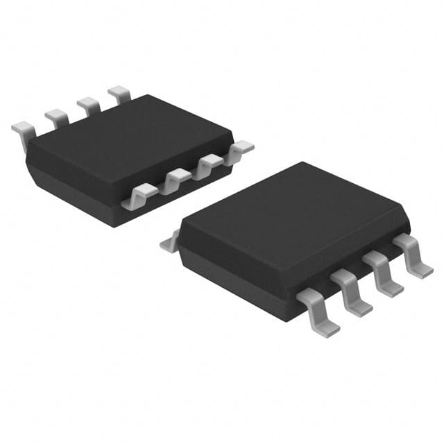
The Renesas ICS553MI is a fanout buffer designed for clock distribution applications. It accepts a single clock input and provides four outputs, maintaining a 1:4 ratio. This device operates at frequencies up to 200 MHz and utilizes CMOS technology for both its input and output signals.
The ICS553MI supports a wide operating voltage range from 2.375V to 5.25V, making it versatile for various system designs. It is specified for operation across an industrial temperature range of -40°C to 85°C. The buffer is packaged in an 8-SOIC form factor, suitable for surface mount assembly.
This clock buffer is designed for applications requiring reliable clock signal distribution. Its surface mount package and broad operating conditions make it adaptable for integration into a wide array of electronic systems.
The operating voltage range for the ICS553MI is 2.375V to 5.25V.
The ICS553MI supports a maximum frequency of 200 MHz.
The ICS553MI uses CMOS input and CMOS output signals.
The operating temperature range for the ICS553MI is -40°C to 85°C.
The ICS553MI is available in an 8-SOIC package.