

| Distributor | Stock | Pricing | MOQ | PKG | Lead Time | Date Code | On Order Quantity | On Order Delivery | |
|---|---|---|---|---|---|---|---|---|---|
|
9,562 pcs
|
9562 pcs | On Request | 1 | On Request | On Request | On Request | On Request | On Request | |
|
7,379 pcs
|
7379 pcs | On Request | 1 | On Request | On Request | On Request | On Request | On Request |
| Category | |
| Manufacturer Name | |
| Mounting Type | |
| Number of I | |
| Number of LABs | |
| Number of Logic Elements | |
| Operating Temperature | |
| Supplier Device Package | |
| Supplier Package | |
| Total RAM Bits | |
| Voltage |
The Lattice Semiconductor ICE40HX8K-CT256 is an ultra-low power FPGA from the iCE40 family, featuring 7680 LUTs and 206 I/O pins. This device includes 131072 bits of embedded block RAM and operates within a voltage range of 1.14V to 1.26V. It is designed for flexible logic implementation and efficient power consumption.
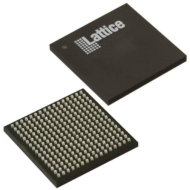
The FPGA is housed in a 256-CABGA package with a 14x14 mm footprint, suitable for surface mount applications. The operating temperature range is -40°C to 100°C (TJ). This device supports various interfaces and offers programmable I/O buffers, making it adaptable for diverse electronic designs.
Key features include a flexible logic architecture, ultra-low power consumption, and embedded memory. The device is configured via SPI or internal Nonvolatile Configuration Memory (NVCM). Its broad range of package options, including small footprint variants, makes it suitable for space-constrained applications. The iCE40 family utilizes an advanced 40nm low power process.
The ICE40HX8K-CT256 has 7680 logic elements.
The ICE40HX8K-CT256 offers 206 I/O pins.
The operating voltage range for the ICE40HX8K-CT256 is 1.14V to 1.26V.
The ICE40HX8K-CT256 is supplied in a 256-CABGA (14x14) package.
The operating temperature range is -40°C to 100°C (TJ).
The ICE40HX8K-CT256 has a total of 131072 bits of RAM.
The ICE40HX8K-CT256 has 960 LABs.