

| Distributor | Stock | Pricing | MOQ | PKG | Lead Time | Date Code | On Order Quantity | On Order Delivery | |
|---|---|---|---|---|---|---|---|---|---|
|
35,190 pcs
|
35190 pcs | On Request | 1 | On Request | On Request | 12+ | On Request | On Request | |
|
1,000 pcs
|
1000 pcs | On Request | 1 | On Request | On Request | On Request | On Request | On Request |
| Category | |
| Manufacturer Name | |
| AEC Qualified | |
| Automotive Grade | |
| Current | |
| DC Current Gain (hFE) (Min) @ Ic, Vce | |
| Halogen Free | |
| Industrial Grade | |
| Medical Grade | |
| Military Grade | |
| Mounting Type | |
| Operating Temperature | |
| Power | |
| Storage Temperature | |
| Supplier Device Package | |
| Tape & Reel | |
| Transistor Type | |
| Vce Saturation (Max) @ Ib, Ic | |
| Voltage |
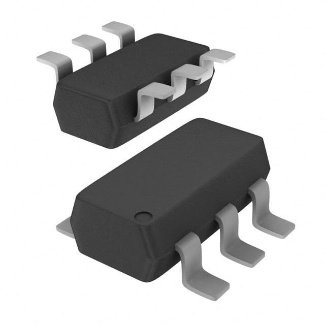
The HN1B01FDW1T1G is a complementary dual general purpose amplifier transistor from onsemi, combining one NPN and one PNP transistor in a single SC-74 (SOT-457) surface mount package. This device is designed for general purpose amplification and switching applications requiring both transistor polarities in a compact footprint.
Key electrical specifications include a maximum collector-emitter voltage (VCEO) of 50V, a maximum collector-base voltage (VCBO) of 60V, and a maximum emitter-base voltage (VEBO) of 7V. The continuous collector current rating is 200mA, with a maximum power dissipation of 380mW. The DC current gain (hFE) is a minimum of 200 at Ic=2mA and Vce=6V, and the collector-emitter saturation voltage is 300mV maximum for the PNP transistor at Ib=10mA and Ic=100mA (250mV for the NPN).
The device operates over a junction temperature range of -55°C to 150°C and is rated for a storage temperature range of -55°C to +150°C. It is surface mountable and comes in the SC-74 package, which is also known as SOT-457. The part is Pb-Free, Halogen Free/BFR Free, and RoHS compliant, with a moisture sensitivity level of 1.
This complementary transistor array is suitable for use in a variety of general purpose amplifier and switching circuits where both NPN and PNP devices are needed. The integration of both transistors in one package helps reduce board space and component count. An automotive qualified variant, SHN1B01FDW1T1G, is also available for applications requiring AEC-Q101 qualification.
| Qty | Low | High |
|---|---|---|
| 1+ | $0.30 | $0.30 |
| 10+ | $0.19 | $0.19 |
| 100+ | $0.12 | $0.12 |
| 500+ | $0.09 | $0.09 |
| 1,000+ | $0.08 | $0.08 |
| 3,000+ | $0.08 | $0.08 |
Estimated market price range - modelled values for guidance only, not live distributor offers.
The maximum collector-emitter voltage (VCEO) is 50V.
The maximum continuous collector current is 200mA.
The package is SC-74 (SOT-457), a surface mount package.
The junction temperature range is -55°C to 150°C.
Yes, the device is RoHS compliant and also Pb-Free and Halogen Free/BFR Free.
The minimum DC current gain (hFE) is 200 at Ic=2mA and Vce=6V.
The maximum power dissipation is 380mW.