

| Distributor | Stock | Pricing | MOQ | PKG | Lead Time | Date Code | On Order Quantity | On Order Delivery | |
|---|---|---|---|---|---|---|---|---|---|
|
2 pcs
|
2 pcs | On Request | 1 | On Request | On Request | On Request | On Request | On Request |
| Category | |
| Manufacturer Name | |
| Differential | |
| Divider | |
| Frequency | |
| Input | |
| Mounting Type | |
| Number of Circuits | |
| Operating Temperature | |
| Output | |
| PLL | |
| Ratio | |
| Supplier Device Package | |
| Tape & Reel | |
| Voltage |
The HMC7043LP7FE from Analog Devices is a high-performance clock buffer featuring a maximum output frequency of 3.2 GHz. This device is designed for ultralow phase noise reference distribution, particularly for high-speed data converters with serial interfaces like JESD204B. It supports up to 14 LVDS, LVPECL, or CML type device clocks (DCLKs) and offers programmable delay on each output channel.
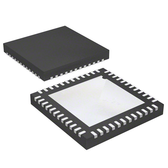
With a wide operating voltage range of 3.135V to 3.465V and an operating temperature range of -40°C to 85°C, the HMC7043LP7FE is suitable for demanding applications. It features a 1:14 output-to-input ratio and supports differential signaling. The device is housed in a 48-lead LFCSP package, suitable for surface mount applications.
Key features include low additive jitter of less than 15 fs rms and a very low noise floor of -155.2 dBc/Hz. The HMC7043LP7FE is also compatible with JESD204B system reference (SYSREF) pulses and supports deterministic synchronization of multiple devices. Its applications include cellular infrastructure, data converter clocking, and phase array reference distribution.
The maximum output frequency for the CLKOUTx/CLKOUTx and SCLKOUTx/SCLKOUTx signals is 3200 MHz.
The HMC7043LP7FE supports CML, LVDS, and LVPECL output types.
The operating voltage range is from 3.135V to 3.465V.
The device operates within a temperature range of -40°C to 85°C.
The HMC7043LP7FE is supplied in a 48-lead LFCSP (7x7) package suitable for surface mounting.
The additive jitter is less than 15 fs rms at 2457.6 MHz (12 kHz to 20 MHz).
The noise floor is very low, measuring -155.2 dBc/Hz at 983.04 MHz.