

| Distributor | Stock | Pricing | MOQ | PKG | Lead Time | Date Code | On Order Quantity | On Order Delivery | |
|---|---|---|---|---|---|---|---|---|---|
|
2,381 pcs
|
2381 pcs | On Request | 1 | On Request | On Request | 206 | On Request | On Request |
| Category | |
| Manufacturer Name | |
| Differential | |
| Input | |
| Lead Spacing | |
| Mounting Type | |
| Number of Circuits | |
| Operating Temperature | |
| Operating Voltage | |
| Output | |
| Ratio | |
| Supplier Device Package | |
| Tape & Reel | |
| Type | |
| Voltage |
The GTLP6C816MTCX from ON Semiconductor is a high-speed clock driver that facilitates signal level translation between TTL and GTLP logic. This device is engineered to provide a robust interface for systems requiring communication between cards operating at TTL logic levels and a backplane operating at GTLP logic levels.
Key electrical characteristics include a supply voltage range of 4.75V to 5.25V and an operating temperature range of -40°C to 85°C. The GTLP6C816MTCX features a 1:6 fanout for the TTL port and a 1:2 fanout for the GTLP port, supporting efficient signal distribution. It is designed with edge rate control circuitry to minimize output noise on the GTLP port and includes PVT compensation for consistent performance across process, voltage, and temperature variations.
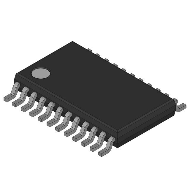
This component is housed in a 24-TSSOP package, suitable for surface mounting. The device supports both TTL and GTLP input signal types and provides GTLP and TTL outputs. Its design incorporates features like bushold data inputs and power-up/down high impedance for live insertion capabilities, making it a reliable choice for high-speed backplane applications.
The supply voltage range is 4.75V to 5.25V.
The operating temperature range is -40°C to 85°C.
It is available in a 24-TSSOP package.
It provides a 1:6 fanout for the TTL port and a 1:2 fanout for the GTLP port.
Yes, it supports both GTLP and TTL input signal types.