

| Distributor | Stock | Pricing | MOQ | PKG | Lead Time | Date Code | On Order Quantity | On Order Delivery | |
|---|---|---|---|---|---|---|---|---|---|
|
102,000 pcs
|
102000 pcs | On Request | 1 | On Request | On Request | On Request | On Request | On Request |
| Category | |
| Manufacturer Name | |
| Configuration | |
| Current | |
| Drain to Source Voltage (Vdss) | |
| Gate Charge (Qg) (Max) @ Vgs | |
| Mounting Type | |
| Operating Temperature | |
| Power | |
| Rds On (Max) @ Id, Vgs | |
| Supplier Device Package | |
| Technology | |
| Vgs(th) (Max) @ Id |
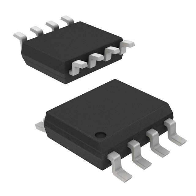
The FQS4900TF is a dual N and P-Channel MOSFET array from On Semiconductor, designed for a variety of switching and power management applications. The N-Channel MOSFET offers a maximum drain-source voltage of 60V and a continuous drain current of 1.3A, while the P-Channel MOSFET provides a higher voltage rating of 300V with a 300mA continuous drain current.
Both channels feature a maximum Rds(on) of 550mOhm (tested at 650mA and 10V gate drive for the N-Channel). The device has a maximum gate charge of 2.1nC at 5V and a maximum gate threshold voltage of 1.95V at 20mA drain current. Total package power dissipation is rated at 2W.
The device is housed in a compact 8-SOIC surface mount package with an operating junction temperature range of -55°C to 150°C. Tape and reel packaging is available for automated assembly. This MOSFET array is suitable for high-density circuit designs requiring both N and P-Channel devices in a single package to simplify layout and reduce component count.
| Qty | Low | High |
|---|---|---|
| 3,000+ | $0.51 | $0.51 |
| 6,000+ | $0.48 | $0.48 |
Estimated market price range - modelled values for guidance only, not live distributor offers.
The N-Channel MOSFET is rated at 60V, and the P-Channel at 300V.
The N-Channel can handle 1.3A continuous, while the P-Channel is rated at 300mA.
It comes in an 8-SOIC surface mount package (0.154", 3.90mm width).
The junction temperature range is -55°C to 150°C.
The maximum Rds(on) is 550mOhm at Id=650mA and Vgs=10V, likely for the N-Channel.
RoHS3 compliant according to existing database records (unverified).
The total package power dissipation is 2W.