

| Distributor | Stock | Pricing | MOQ | PKG | Lead Time | Date Code | On Order Quantity | On Order Delivery | |
|---|---|---|---|---|---|---|---|---|---|
|
200 pcs
|
200 pcs | On Request | 1 | On Request | On Request | 10+ | On Request | On Request |
| Category | |
| Manufacturer Name | |
| Current | |
| Drain to Source Voltage (Vdss) | |
| Drive Voltage (Max Rds On, Min Rds On) | |
| FET Type | |
| Gate Charge (Qg) (Max) @ Vgs | |
| Input Capacitance (Ciss) (Max) @ Vds | |
| Mounting Type | |
| Operating Temperature | |
| Power Dissipation (Max) | |
| Rds On (Max) @ Id, Vgs | |
| Supplier Device Package | |
| Technology | |
| Vgs (Max) | |
| Vgs(th) (Max) @ Id |
The FQPF4N90 is a 900V N-Channel enhancement mode power MOSFET produced using Fairchild Semiconductor's proprietary planar stripe DMOS technology. It is designed to minimize on-state resistance, provide superior switching performance, and withstand high energy pulses in avalanche and commutation mode.
Key electrical specifications include a drain-source voltage rating of 900V, continuous drain current of 2.5A at 25°C case temperature, and maximum on-resistance of 3.3 Ω at VGS = 10V and ID = 1.25A. The device offers low gate charge (typically 24 nC) and low reverse transfer capacitance (typically 9.5 pF) for efficient high-frequency switching.
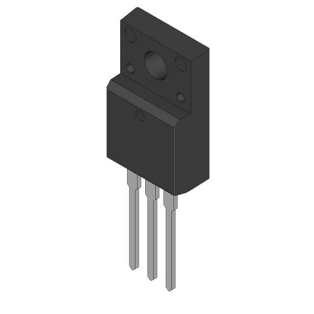
The FQPF4N90 is packaged in a TO-220F full pack (TO-220-3) through-hole package, with a junction-to-case thermal resistance of 2.66 °C/W. The MOSFET is 100% avalanche tested and capable of single pulsed avalanche energy up to 570 mJ.
This device is well suited for high efficiency switch mode power supplies and other applications requiring high voltage switching with low conduction losses. The operating junction temperature range is -55°C to 150°C.
The maximum drain-source voltage (Vdss) is 900 V.
The FQPF4N90 is packaged in a TO-220-3 Full Pack (TO-220F-3) through-hole package.
The operating junction temperature range is -55°C to 150°C.
The existing data indicates RoHS3 Compliant status, but this is unverified. Official compliance documentation should be obtained from the manufacturer.
The drain-source on-resistance is typically 2.7 Ω and maximum 3.3 Ω at VGS = 10 V and ID = 1.25 A.
The maximum continuous drain current is 2.5 A at a case temperature of 25°C, and 1.58 A at 100°C.