


| Distributor | Stock | Pricing | MOQ | PKG | Lead Time | Date Code | On Order Quantity | On Order Delivery | |
|---|---|---|---|---|---|---|---|---|---|
|
1,000 pcs
|
1000 pcs | On Request | 1 | On Request | On Request | On Request | On Request | On Request |
| Category | |
| Manufacturer Name | |
| Current | |
| Drain to Source Voltage (Vdss) | |
| Drive Voltage (Max Rds On, Min Rds On) | |
| FET Type | |
| Gate Charge (Qg) (Max) @ Vgs | |
| Input Capacitance (Ciss) (Max) @ Vds | |
| Mounting Type | |
| Operating Temperature | |
| Power Dissipation (Max) | |
| Rds On (Max) @ Id, Vgs | |
| Supplier Device Package | |
| Technology | |
| Vgs (Max) | |
| Vgs(th) (Max) @ Id |
The FQN1N50CTA is an N-Channel MOSFET from ON Semiconductor designed for low-power switching and signal amplification applications. It features a drain-source voltage rating of 500V and a continuous drain current of 380mA. The device offers a maximum on-resistance of 6 Ohms at 190mA and 10V gate-source drive, with a gate charge of 6.4 nC and input capacitance of 195 pF.
This MOSFET is suitable for circuits requiring high voltage capability in a compact through-hole package. The threshold voltage is 4V maximum at 250µA, and the recommended drive voltage is 10V. Maximum power dissipation is 890mW at ambient temperature and 2.08W at case temperature.
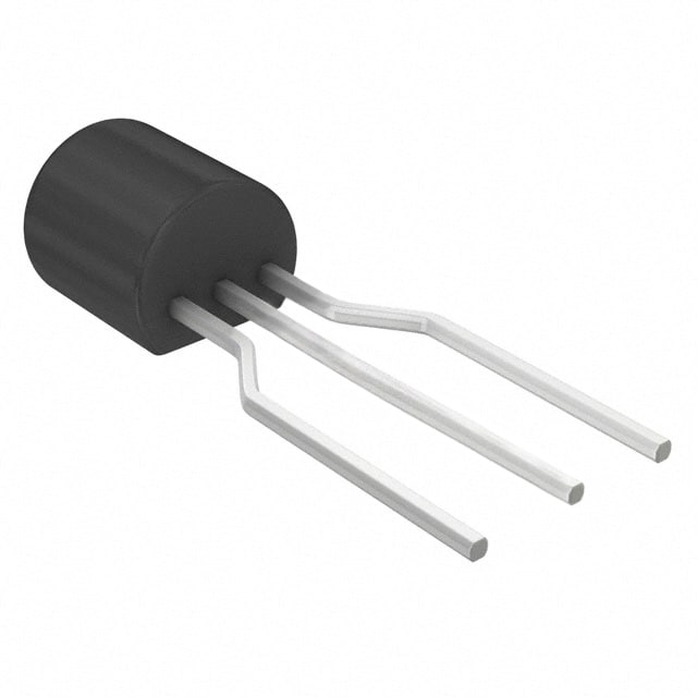
The FQN1N50CTA is housed in a TO-92-3 package (also known as TO-226-3 with formed leads) and is designed for through-hole mounting. It operates over a junction temperature range of -55°C to 150°C. The device is listed as RoHS3 compliant (unverified).
500V.
TO-92-3 through-hole package.
-55°C to 150°C.
Yes, it is listed as RoHS3 Compliant (unverified).
6 Ohm maximum at 190mA and 10V gate-source voltage.
6.4 nC maximum at 10V gate-source voltage.
195 pF maximum at 25V drain-source voltage.