

| Distributor | Stock | Pricing | MOQ | PKG | Lead Time | Date Code | On Order Quantity | On Order Delivery | |
|---|---|---|---|---|---|---|---|---|---|
|
18,520 pcs
|
18520 pcs | On Request | 1 | On Request | On Request | On Request | On Request | On Request | |
|
720 pcs
|
720 pcs | On Request | 1 | On Request | On Request | On Request | On Request | On Request | |
|
715 pcs
|
715 pcs | On Request | 1 | On Request | On Request | On Request | On Request | On Request |
| Category | |
| Manufacturer Name | |
| Current | |
| Drain to Source Voltage (Vdss) | |
| Drive Voltage (Max Rds On, Min Rds On) | |
| FET Type | |
| Gate Charge (Qg) (Max) @ Vgs | |
| Input Capacitance (Ciss) (Max) @ Vds | |
| Mounting Type | |
| Operating Temperature | |
| Power Dissipation (Max) | |
| Rds On (Max) @ Id, Vgs | |
| Supplier Device Package | |
| Tape & Reel | |
| Technology | |
| Vgs (Max) | |
| Vgs(th) (Max) @ Id |
The FQD8P10TM-F085 is a P-Channel enhancement-mode power MOSFET manufactured by onsemi using proprietary planar stripe DMOS technology. This device is rated for a maximum drain-source voltage of -100V and a continuous drain current of -6.6A at 25°C case temperature, with pulsed drain current capability up to -26.4A. The on-resistance is specified at a maximum of 530mΩ when driven with a gate-source voltage of -10V and a drain current of 3.3A.
This MOSFET features low gate charge (12nC typical) and low reverse transfer capacitance (30pF typical), enabling fast switching performance suitable for high-efficiency power conversion circuits. The device is 100% avalanche tested and offers improved dv/dt capability, with a single pulsed avalanche energy rating of 150mJ and a peak diode recovery dv/dt of -6.0V/ns. It is qualified to AEC-Q101 for automotive applications.
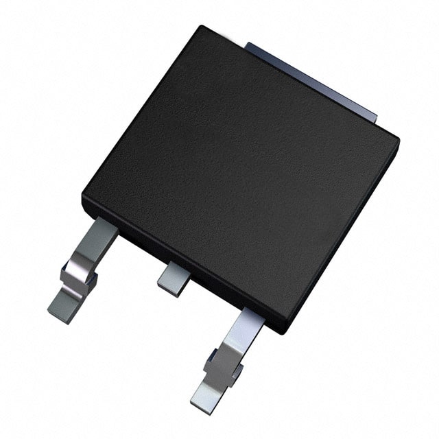
The device is available in a TO-252-3 (DPAK) surface-mount package with a supplier device package designation of TO-252AA. It supports a wide operating junction temperature range from -55°C to +150°C. Power dissipation is rated at 44W at 25°C case temperature and 2.5W at 25°C ambient temperature. The component is RoHS compliant and lead-free (Pb-Free).
Typical applications include audio amplifiers, high-efficiency switching DC/DC converters, and DC motor control circuits, where the P-Channel configuration simplifies drive circuitry in low-side switching applications.
The maximum drain-source voltage (VDSS) is -100V.
The continuous drain current is -6.6A at TC=25°C and -4.2A at TC=100°C. Pulsed drain current is -26.4A.
The maximum on-resistance (RDS(on)) is 530mΩ at ID=3.3A and VGS=-10V.
The operating junction temperature range is -55°C to +150°C.
Yes, the device is RoHS compliant and lead-free (Pb-Free) as stated in the datasheet.
The device is available in a TO-252-3 (DPAK) surface-mount package with supplier device package TO-252AA.
The maximum gate threshold voltage (VGS(th)) is 4V at ID=250µA.