

| Distributor | Stock | Pricing | MOQ | PKG | Lead Time | Date Code | On Order Quantity | On Order Delivery | |
|---|---|---|---|---|---|---|---|---|---|
|
761 pcs
|
761 pcs | On Request | 1 | On Request | On Request | On Request | On Request | On Request |
| Category | |
| Manufacturer Name | |
| Current | |
| Drain to Source Voltage (Vdss) | |
| Drive Voltage (Max Rds On, Min Rds On) | |
| FET Type | |
| Gate Charge (Qg) (Max) @ Vgs | |
| Input Capacitance (Ciss) (Max) @ Vds | |
| Mounting Type | |
| Operating Temperature | |
| Power Dissipation (Max) | |
| Rds On (Max) @ Id, Vgs | |
| Supplier Device Package | |
| Technology | |
| Termination Style | |
| Vgs (Max) | |
| Vgs(th) (Max) @ Id |
The FQD5N50CTM-WS is a 500V, 4A N-Channel enhancement mode power MOSFET from On Semiconductor, part of the FQD5N50C series. It is designed for high efficiency switched mode power supplies, active power factor correction, and electronic lamp ballasts based on half bridge topology.
This MOSFET features a maximum drain-source on-resistance of 1.4Ohm at VGS=10V and ID=2A, with a typical gate charge of 18nC. It is rated for a maximum power dissipation of 48W at case temperature 25°C and 2.5W at ambient temperature. The device is 100% avalanche tested and offers improved dv/dt capability.
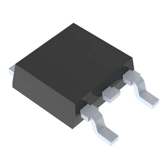
The FQD5N50CTM-WS is housed in a TO-252 (DPak) surface mount package with gull wing leads. It operates over a junction temperature range of -55°C to 150°C.
The drain-source voltage rating is 500V.
The continuous drain current is 4A at a case temperature of 25°C.
The package is TO-252-3, DPak (2 Leads + Tab), SC-63, with a supplier device package of TO-252 (D-Pak).
The operating junction temperature range is -55°C to 150°C.
The datasheet indicates the device is RoHS compliant.
The maximum drain-source on-resistance is 1.4Ohm at VGS=10V and ID=2A.
The maximum gate charge is 24nC at VGS=10V.