

| Distributor | Stock | Pricing | MOQ | PKG | Lead Time | Date Code | On Order Quantity | On Order Delivery | |
|---|---|---|---|---|---|---|---|---|---|
|
50,400 pcs
|
50400 pcs | On Request | 1 | On Request | On Request | On Request | On Request | On Request | |
|
175 pcs
|
175 pcs | On Request | 1 | On Request | On Request | On Request | On Request | On Request |
| Category | |
| Manufacturer Name | |
| Current | |
| Drain to Source Voltage (Vdss) | |
| Drive Voltage (Max Rds On, Min Rds On) | |
| FET Type | |
| Gate Charge (Qg) (Max) @ Vgs | |
| Input Capacitance (Ciss) (Max) @ Vds | |
| Mounting Type | |
| Operating Temperature | |
| Power Dissipation (Max) | |
| Rds On (Max) @ Id, Vgs | |
| Supplier Device Package | |
| Technology | |
| Vgs (Max) | |
| Vgs(th) (Max) @ Id |
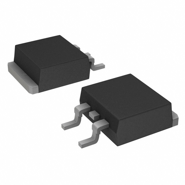
The FQB7P20TM is a P-Channel MOSFET manufactured by ON Semiconductor. It features a drain-source voltage (Vdss) of 200V and a continuous drain current (Id) of 7.3A at 25°C case temperature. The on-resistance (Rds(on)) is 690 mOhm maximum at a gate-source voltage of 10V and drain current of 3.65A. The gate threshold voltage (Vgs(th)) is 5V maximum at 250µA. Total gate charge (Qg) is 25 nC maximum at 10V, and input capacitance (Ciss) is 770 pF maximum at Vds = 25V. Power dissipation is rated at 90W maximum at case temperature (Tc) and 3.13W at ambient temperature (Ta). The device operates over a junction temperature range of -55°C to 150°C. It is offered in a surface mount D²PAK (TO-263) package, suitable for automated assembly. The part is listed as RoHS3 compliant, though this status is unverified.
200V.
Surface mount D2PAK (TO-263) package.
-55°C to 150°C (junction).
RoHS3 compliant (unverified).
5V max at 250µA.
690 mOhm max at 3.65A, 10V.
25 nC max at 10V.