

| Distributor | Stock | Pricing | MOQ | PKG | Lead Time | Date Code | On Order Quantity | On Order Delivery | |
|---|---|---|---|---|---|---|---|---|---|
|
133 pcs
|
133 pcs | On Request | 1 | On Request | On Request | On Request | On Request | On Request |
| Category | |
| Manufacturer Name | |
| AEC Qualified | |
| Automotive Grade | |
| Current | |
| Drain to Source Voltage (Vdss) | |
| Drive Voltage (Max Rds On, Min Rds On) | |
| FET Type | |
| Gate Charge (Qg) (Max) @ Vgs | |
| Halogen Free | |
| Industrial Grade | |
| Input Capacitance (Ciss) (Max) @ Vds | |
| Lead Style | |
| Medical Grade | |
| Military Grade | |
| Mounting Type | |
| Operating Temperature | |
| Power Dissipation (Max) | |
| Rds On (Max) @ Id, Vgs | |
| SVHC Present | |
| Supplier Device Package | |
| Technology | |
| Vgs (Max) | |
| Vgs(th) (Max) @ Id |
The FQA6N90C-F109 is an N-channel enhancement mode power MOSFET from ON Semiconductor, part of the QFET family. It is rated for a maximum drain-source voltage of 900 V and a continuous drain current of 6.0 A at TC=25°C (3.87 A at TC=100°C). The device features a maximum on-resistance of 2.3 Ω at VGS=10V and ID=3A, with a typical on-resistance of 1.93 Ω.
Designed for high-voltage switching, the MOSFET has a typical gate charge of 30 nC and a typical reverse transfer capacitance of 11 pF. It is 100% avalanche tested and supports a single-pulse avalanche energy of 650 mJ and repetitive avalanche energy of 19.8 mJ. Maximum power dissipation is 198 W at TC=25°C.
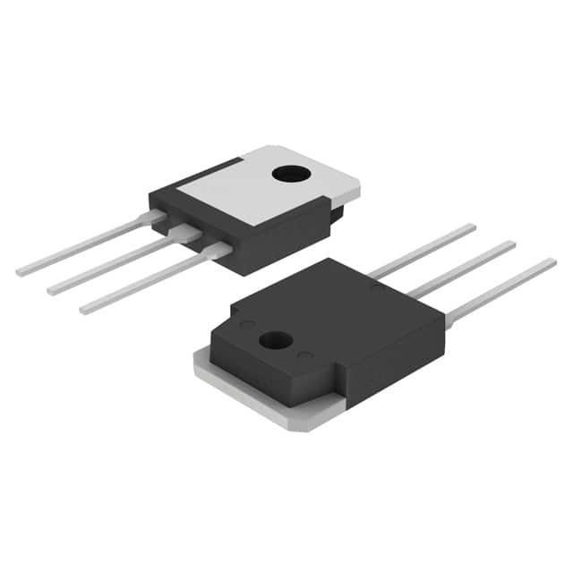
The FQA6N90C-F109 is housed in a through-hole TO-3PN package (TO-3P-3, SC-65-3) and operates over a junction temperature range of -55°C to +150°C. Thermal resistance from junction to case is 0.63 °C/W maximum. The device is RoHS compliant and supplied in tubes of 30 units.
Typical applications include switched mode power supplies, active power factor correction (PFC), and electronic lamp ballasts.
The maximum drain-source voltage (Vdss) is 900 V.
The through-hole TO-3PN package (also listed as TO-3P-3, SC-65-3).
The junction operating temperature range is -55°C to +150°C.
The product is listed as RoHS compliant (RoHS3) in the supplier data, though compliance is not independently verified.
The maximum continuous drain current is 6.0 A at TC=25°C, derated to 3.87 A at TC=100°C.
Maximum RDS(on) is 2.3 Ω at VGS=10V, ID=3A; typical is 1.93 Ω.
Maximum power dissipation is 198 W at TC=25°C.