

| Distributor | Stock | Pricing | MOQ | PKG | Lead Time | Date Code | On Order Quantity | On Order Delivery | |
|---|---|---|---|---|---|---|---|---|---|
|
1,000 pcs
|
1000 pcs | On Request | 1 | On Request | On Request | On Request | On Request | On Request | |
|
570 pcs
|
570 pcs | On Request | 1 | On Request | On Request | On Request | On Request | On Request |
| Category | |
| Manufacturer Name | |
| Approval Agency | |
| Common Mode Transient Immunity (Min) | |
| Current | |
| Lead Spacing | |
| Mounting Type | |
| Number of Channels | |
| Operating Temperature | |
| Propagation Delay tpLH | |
| Pulse Width Distortion (Max) | |
| Rise | |
| Supplier Device Package | |
| Supplier Package | |
| Technology | |
| Voltage |
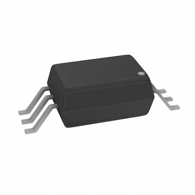
The ON Semiconductor FOD8343TR2 is a high-speed gate drive optocoupler in a stretched body SOP 6-pin package. It is designed to drive medium-power IGBT and MOSFET devices, making it suitable for fast-switching applications in motor-control inverters and high-performance power systems.
This optocoupler offers a maximum peak output current of 4.0A and a minimum common mode rejection of 50kV/µs. It operates with a supply voltage range of 10V to 30V and features fast switching speeds with a maximum propagation delay of 210ns and a maximum pulse width distortion of 65ns. The device is housed in a 6-SOIC surface mount package.
Key features include 8mm creepage and clearance distances for reliable high-voltage insulation and an extended industrial temperature range of -40°C to 100°C. Safety and regulatory approvals include UL1577 and DIN EN/IEC60747-5-5.
Applications include AC and brushless DC motor drives, industrial inverters, uninterruptible power supplies, induction heating, and isolated IGBT/Power MOSFET gate drives.
| Qty | Low | High |
|---|---|---|
| 1+ | $2.55 | $2.55 |
Estimated market price range - modelled values for guidance only, not live distributor offers.
The FOD8343TR2 has a maximum peak output current of 4.0 A.
The operating supply voltage range is 10 V to 30 V.
The operating temperature range is -40°C to 100°C.
The FOD8343TR2 is supplied in a 6-SOIC (0.268", 6.80mm Width) surface mount package.
The minimum common mode transient immunity is 50 kV/µs.
The maximum propagation delay is 210 ns, and the maximum pulse width distortion is 65 ns.