

| Distributor | Stock | Pricing | MOQ | PKG | Lead Time | Date Code | On Order Quantity | On Order Delivery | |
|---|---|---|---|---|---|---|---|---|---|
|
19 pcs
|
19 pcs | On Request | 1 | On Request | On Request | On Request | On Request | On Request |
| Category | |
| Manufacturer Name | |
| Data Rate | |
| Mounting Type | |
| Number of Drivers | |
| Operating Temperature | |
| Propagation Delay | |
| Protocol | |
| Supplier Device Package | |
| Supplier Package | |
| Type | |
| Voltage |
The FIN1047MTC from On Semiconductor is a quad driver utilizing Low Voltage Differential Signaling (LVDS) technology. This device translates LVTTL signal levels to LVDS levels, offering a typical differential output swing of 350mV. It is designed for high-speed transfer of clock and data, providing low EMI at ultra-low power dissipation even at high frequencies.
Key features include a data rate greater than 400Mbps, a flow-through pinout that simplifies PCB layout, and 3.3V power supply operation. The driver exhibits a maximum differential pulse skew of 0.4 ns and a maximum propagation delay of 1.7 ns. It meets or exceeds the TIA/EIA-644 LVDS standard and is pin compatible with equivalent RS-422 and LVPECL devices.
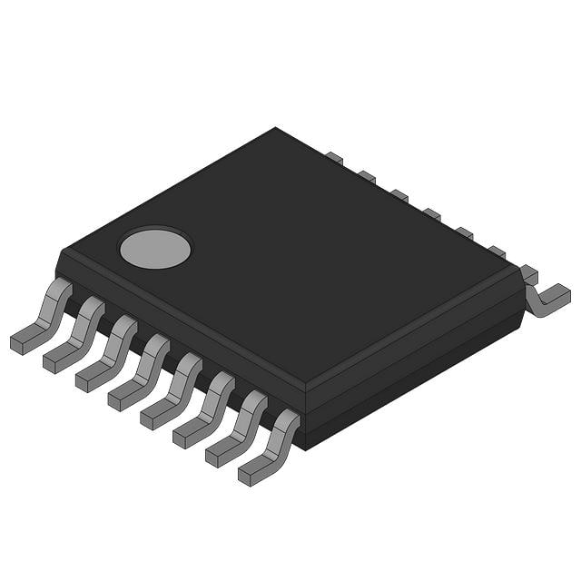
This component is available in a 16-lead TSSOP package, which saves space. The operating temperature range is -40°C to 85°C. The FIN1047MTC can be paired with its companion receiver, the FIN1048, or any other LVDS receiver for system integration.
The FIN1047MTC operates from 3V to 3.6V.
The FIN1047MTC is supplied in a 16-TSSOP package.
The operating temperature range for the FIN1047MTC is -40°C to 85°C.
The FIN1047MTC supports data rates greater than 400Mbps.
The FIN1047MTC uses LVDS protocol.