

| Distributor | Stock | Pricing | MOQ | PKG | Lead Time | Date Code | On Order Quantity | On Order Delivery | |
|---|---|---|---|---|---|---|---|---|---|
|
2,000 pcs
|
2000 pcs | On Request | 1 | On Request | On Request | On Request | On Request | On Request |
| Category | |
| Manufacturer Name | |
| Data Rate | |
| Duplex | |
| Lead Spacing | |
| Mounting Type | |
| Number of Drivers | |
| Operating Temperature | |
| Propagation Delay | |
| Protocol | |
| Supplier Device Package | |
| Supplier Package | |
| Type | |
| Voltage |
The FIN1019MTC is a high-speed differential driver/receiver pair from ON Semiconductor, utilizing Low Voltage Differential Signaling (LVDS) technology. This transceiver is designed for high-speed interconnects and supports data rates greater than 400Mbps.
Key electrical specifications include a 3.3V power supply operation, a maximum differential pulse skew of 0.5ns, and a maximum propagation delay of 2.5ns. The receiver offers a sensitivity of 100mV, while the driver provides a typical differential output swing of 350mV. It operates over a temperature range of -40°C to 85°C.
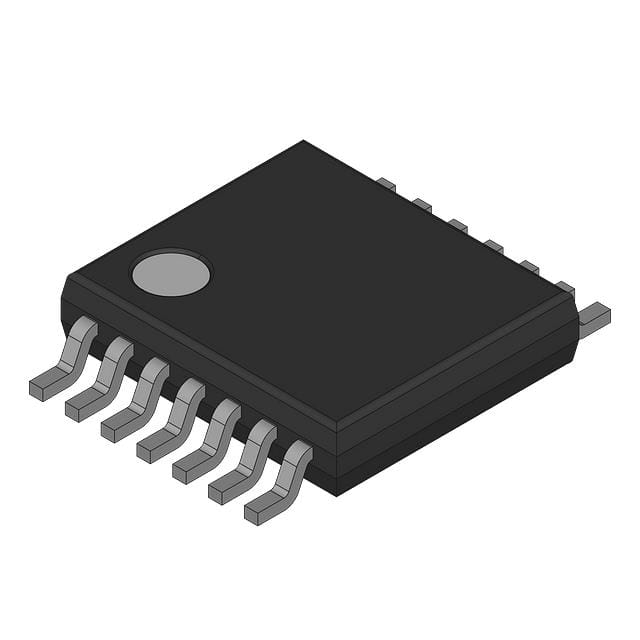
This device is housed in a 14-TSSOP package with a surface mount type, simplifying PCB layout with its flow-through pinout. The FIN1019MTC meets or exceeds the TIA/EIA-644 LVDS standard and offers features such as power-off protection and fail-safe protection for open-circuit, shorted, and terminated conditions.
The FIN1019MTC operates on a 3.3V power supply, with a range of 3V to 3.6V.
The FIN1019MTC is available in a 14-TSSOP package.
The operating temperature range for the FIN1019MTC is -40°C to 85°C.
The FIN1019MTC transceiver supports data rates greater than 400Mbps.
The FIN1019MTC uses the LVDS protocol.