Ready to onboard?
Are you ready to join DistyParts and
grow your business?


| Distributor | Stock | Pricing | MOQ | PKG | Lead Time | Date Code | On Order Quantity | On Order Delivery | |
|---|---|---|---|---|---|---|---|---|---|
|
102,000 pcs
|
102000 pcs | On Request | 1 | On Request | On Request | 04+ | On Request | On Request |
| Category | |
| Manufacturer Name | |
| Collector Cut-Off Current (ICES) | |
| Collector-Emitter Breakdown Voltage (BVCES) | |
| Current | |
| Fall Time (tf) | |
| Gate-Emitter Leakage Current (IGES) | |
| Gate-Emitter Threshold Voltage (Vge(th)) | |
| Gate-Emitter Voltage (VGES) | |
| IGBT Type | |
| Input Capacitance (Cies) | |
| Input Type | |
| Lead Temperature for Soldering | |
| Mounting Type | |
| Operating Temperature | |
| Output Capacitance (Coes) | |
| Power | |
| Reverse Transfer Capacitance (Cres) | |
| Rise Time (tr) | |
| Storage Temperature | |
| Storage Temperature (Tstg) | |
| Supplier Device Package | |
| Thermal Resistance Junction to Ambient (RθJA) | |
| Turn-Off Delay Time (td(off)) | |
| Turn-On Delay Time (td(on)) | |
| Vce(on) (Max) @ Vge, Ic | |
| Voltage |
The FGS15N40LTF is a trench-gate N-channel IGBT designed for high peak current applications such as strobe flash circuits. It offers a collector-emitter voltage rating of 400V and a pulsed collector current of 130A, with a saturation voltage ranging from 2.0V to 8.0V at 4V gate drive.
Electrical characteristics include a gate-emitter threshold voltage of 1.4V max, input capacitance of 3800pF, and switching speeds with turn-on delay of 0.15µs, rise time of 1.5µs, turn-off delay of 0.15µs/0.3µs, and fall time of 1.5µs/3.0µs. The device requires a minimum gate resistor of 15Ω.
The IGBT is housed in a surface-mount 8-SOIC package with a maximum power dissipation of 2W at 25°C ambient when mounted on a PCB. It operates over a junction temperature range of -40°C to 150°C and has a storage temperature range of -40°C to 150°C. The lead temperature for soldering is 300°C for 5 seconds.
| Qty | Low | High |
|---|---|---|
| 3,000+ | $0.44 | $0.44 |
| 6,000+ | $0.41 | $0.41 |
| 9,000+ | $0.41 | $0.41 |
Estimated market price range - modelled values for guidance only, not live distributor offers.
The collector-emitter voltage rating (Vces) is 400V.
The pulsed collector current (Icm) is 130A, pulse width limited by junction temperature.
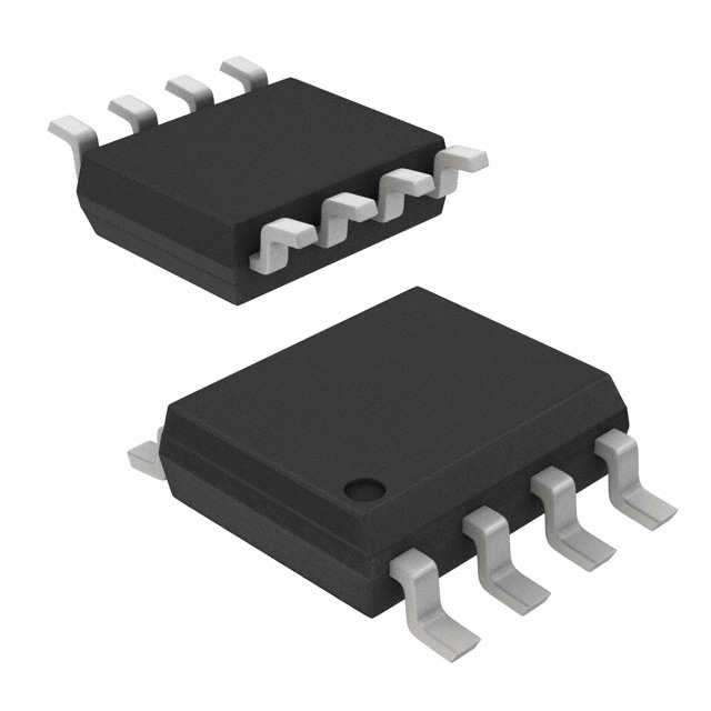
It comes in a surface mount 8-SOIC (0.154", 3.90mm Width) package.
The operating junction temperature range is -40°C to 150°C.
The datasheet indicates RoHS3 compliance, but this status is unverified.
Turn-on delay time is 0.15µs, rise time is 1.5µs, turn-off delay time is 0.15µs (typ) / 0.3µs (max), and fall time is 1.5µs (typ) / 3.0µs (max) under test conditions VCC=300V, IC=130A, VGE=4V, RG=15Ω, resistive load.
The saturation voltage (VCE(sat)) is 2.0V min, 4.5V typical, and 8.0V max at IC=130A and VGE=4V.