

| Distributor | Stock | Pricing | MOQ | PKG | Lead Time | Date Code | On Order Quantity | On Order Delivery | |
|---|---|---|---|---|---|---|---|---|---|
|
2,803 pcs
|
2803 pcs | On Request | 1 | On Request | On Request | 05+ | On Request | On Request | |
|
770 pcs
|
770 pcs | On Request | 1 | On Request | On Request | On Request | On Request | On Request |
| Category | |
| Manufacturer Name | |
| Current | |
| Drain to Source Voltage (Vdss) | |
| Drive Voltage (Max Rds On, Min Rds On) | |
| FET Type | |
| Gate Charge (Qg) (Max) @ Vgs | |
| Input Capacitance (Ciss) (Max) @ Vds | |
| Lead Spacing | |
| Mounting Type | |
| Operating Temperature | |
| Power Dissipation (Max) | |
| Rds On (Max) @ Id, Vgs | |
| Storage Temperature | |
| Supplier Device Package | |
| Tape & Reel | |
| Technology | |
| Termination Style | |
| Vgs (Max) | |
| Vgs(th) (Max) @ Id |
The FDZ206P is a P-Channel MOSFET from On Semiconductor, built with advanced PowerTrench technology. It features a maximum drain-source voltage of 20V and continuous drain current of 13A at 25°C, with pulsed current capability up to 60A. The device offers low on-resistance: 9.5mΩ typical at VGS = -4.5V and 14.5mΩ at VGS = -2.5V, enabling efficient power switching.
Gate threshold voltage ranges from -0.6V to -1.5V, and the device is specified for drive voltages of 2.5V and 4.5V. Input capacitance is 4280pF typical, with gate charge of 53nC at VGS = -4.5V. Switching speeds are characterized with typical turn-on delay of 17ns and turn-off delay of 115ns.
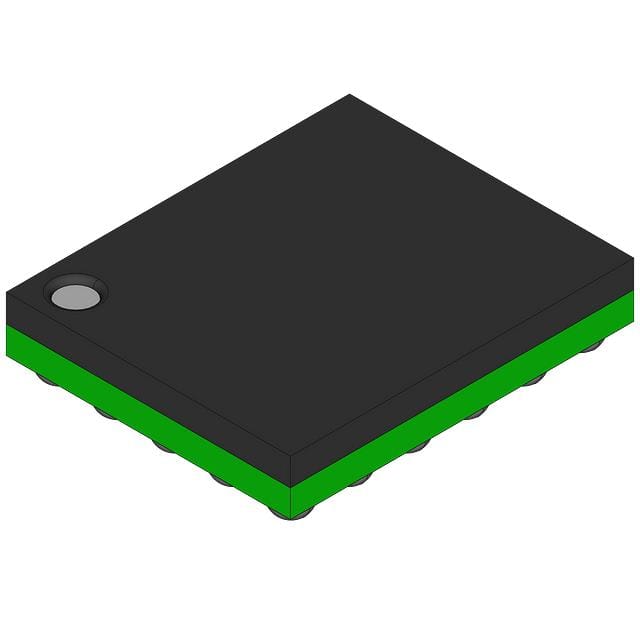
The MOSFET is housed in a 30-WFBGA package (30-BGA 4x3.5mm) with 0.65mm ball pitch and an ultra-thin profile under 0.8mm when mounted. It supports surface mount assembly and is supplied in tape and reel packaging with 4000 units per reel. Thermal resistance junction-to-ambient is 56°C/W, and maximum power dissipation is 2.2W at 25°C ambient.
Typical applications include battery management, load switching, and battery protection circuits where space efficiency and low on-resistance are critical.
20V maximum.
13A at 25°C ambient, continuous.
9.5mΩ maximum at VGS = -4.5V, ID = -13A; 14.5mΩ maximum at VGS = -2.5V, ID = -10.5A.
-55°C to 150°C junction temperature.
30-WFBGA (30-BGA 4x3.5mm) with 0.65mm ball pitch.
RoHS3 compliant (unverified).
Minimum -0.6V, typical -0.9V, maximum -1.5V at VDS = VGS, ID = -250µA.